This article based on video tutorial by prof. Sam Ben-Yaakov explains fundamentals, benefits and design notes related to tapped inductor converters.
Tapped inductor converters are a practical alternative to classical buck converters when you need a low output voltage from a high input voltage and the required duty cycle becomes very small. They use a coupled inductor structure to reduce switch and inductor current stress, improve usability at low duty cycles, and retain some of the energy‑transfer behavior familiar from flyback converters.
Key Takeaways
- Tapped Inductor Buck Converters provide an effective solution for stepping down high input voltages to low output voltages without requiring very small duty cycles.
- They use a coupled inductor structure, improving current stress management during operation compared to classical buck converters.
- The design focuses on selecting the right turns ratio to enhance voltage transfer and manage duty cycle ranges.
- Applications include off-line DC to DC conversion and systems requiring high pulse currents, leveraging their unique characteristics.
- Design engineers should consider aspects like leakage inductance and snubber designs for reliable operation in practical applications.
Key features and benefits
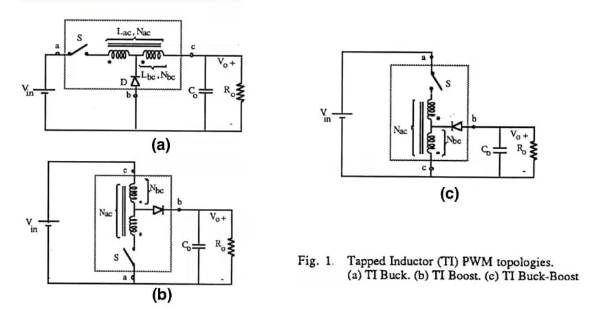
Tapped inductor converters replace the single inductor of a classical buck with a coupled inductor having two windings on the same core. The inductor is “tapped” such that the current and voltage distribution between the two windings changes between on and off intervals of the power switch, which directly impacts device stresses and the effective conversion ratio.
Topology overview
- The tapped inductor buck converter uses two coupled inductors and wound on a common core, a power switch on the input side and a diode on the output side.
- In a conventional buck, a single inductor carries the full output current continuously; in the tapped inductor version, current distribution and conduction intervals differ between the two windings.
- The same tapped inductor idea can be applied to boost and buck‑boost configurations, but the focus here is on the buck version for very small effective duty cycles.
- The structure is closely related to a flyback transformer, but with the windings connected in series so that some energy is delivered to the output already during the switch on‑time.
Voltage transfer and duty cycle behavior
For the tapped inductor buck, the DC conversion ratio can be expressed as a function of the duty cycle and turns ratio. The voltage transfer ratio is given as
where and are the on and off fractions of the switching period and is defined as the ratio between the total number of turns and the number of turns of one section of the inductor.
- For the expression reduces to the classical buck behavior in continuous conduction mode.
- For , the same duty cycle produces a lower output voltage compared to a classical buck.
- To obtain a given low output voltage from a high input, the tapped inductor design can operate at a larger duty cycle than a conventional buck, which is advantageous for control and device stress.
In an example discussed in the presentation, a tapped inductor buck with a 200 V input generates about 25 V output with a duty cycle of approximately 0.5, whereas a classical buck requires a duty cycle around 0.14 for the same operating point. This illustrates how the topology mitigates the challenges of extremely small duty cycles at high step‑down ratios.
Current stress and energy flow
A key motivation for the tapped inductor is the reduction of current stress in both the main switch and a large portion of the inductor.
- In a classical buck, the output inductor carries the full output current continuously, and the switch conducts this full current during its on‑time.
- With a tapped inductor, during the off‑time the series section connected to the switch side effectively sees no current, so a large portion of the inductor is non‑conducting during this interval.
- In the example simulation, the current in the input winding of the tapped inductor reaches about 12 A and conducts only during the on‑time, compared with a continuous inductor current of about 27 A in the classical buck for the same 25 V output from 200 V input.
- The secondary section can experience very high pulse currents, with example peak values around 80 A, which may be useful in applications requiring high current pulses.
This redistribution of current means the switch and part of the magnetic component can be dimensioned for lower RMS current than in an equivalent classical buck design at the same operating point.
Typical applications
Tapped inductor buck converters are particularly attractive where a large step‑down ratio is required and the classical buck would have to run at a very small duty cycle.
- Off‑line or high‑voltage DC to low‑voltage DC conversion, for example from around 200 V DC to tens of volts.
- Point‑of‑load stages following a high‑voltage bus where improved duty‑cycle range and reduced switch current are desired.
- Circuits requiring compressed or pulsed high currents at the output, exploiting the high peak current available in the tapped winding.
- Educational and experimental platforms where designers want to study the relationship between coupled inductors, duty cycle and current stresses.
In many of these use cases, the topology competes with or complements flyback converters, especially where continuous conduction of output current during the switch on‑time is advantageous.
Technical highlights
The video frames the tapped inductor as a coupled magnetic component best represented by an equivalent circuit rather than a simple lumped inductor. A proper understanding of this model is essential for realistic design, especially regarding leakage inductance and snubber requirements.
Magnetic structure and equivalent circuit
- The tapped inductor uses two inductive sections and wound on the same core, with and turns respectively.
- Because inductance scales as the square of the number of turns, the total inductance of the coupled structure is not simply .
- The presentation emphasizes expressing the effective inductance in terms of the total number of turns and a common constant related to the magnetic core, reflecting the dependence.
- For analysis, an equivalent circuit is used with:
- An ideal transformer representing the turns ratio.
- A magnetizing inductance placed on the output side of this ideal transformer.
- Two leakage inductances representing energy stored outside the ideal coupling.
This model is analogous to that used for flyback transformers and is the foundation for deriving a SPICE‑compatible large‑signal model of the converter.
Leakage inductance and snubber behavior
Coupled inductors inevitably exhibit leakage inductance, which leads to stored energy that must be handled when the switch turns off.
- When the switch turns off while current flows in the primary section, the leakage inductance causes a voltage spike across the switch as the current is abruptly interrupted.
- A snubber network across the switch is recommended, similar to flyback converters, to clamp this voltage and dissipate or, in more advanced designs, recover the stored leakage energy.
- The example uses a snubber adjusted so that a 1,200 V device sees about 700 V peak, illustrating practical snubber dimensioning relative to device ratings.
Designers must factor leakage‑related spikes into device selection, snubber design and PCB layout to ensure reliable operation.
Example simulation parameters
The presentation includes a time‑domain simulation that compares a tapped inductor buck to a classical buck under matched output conditions.
- Input voltage: 200 V DC.
- Output voltage: approximately 25 V in both topologies.
- Switching frequency: 50 kHz.
- Tapped inductor buck:
- Duty cycle about 0.5.
- Turns ratio .
- Example inductances: , , consistent with the square of the turns ratio.
- Coupling coefficient assumed as 0.95, which is optimistic but realistic for a tightly wound structure.
- Classical buck:
- Same nominal inductance value as the effective inductance of the tapped structure.
- Duty cycle adjusted to about 0.14 to achieve the same 25 V output.
Despite identical output conditions, the current waveforms and device stresses differ markedly, highlighting the practical impact of the topology choice.
Relationship to flyback converters
The tapped inductor buck converter can be seen as a variation of the flyback topology with series‑connected windings.
- In a flyback converter, all energy transfer occurs during the switch off‑time: energy is stored in the core when the switch is on and released to the output when the switch is off.
- In the tapped inductor buck, some current flows to the output even during the switch on‑time because of the series connection of the windings.
- During off‑time, the stored energy in the magnetizing inductance is delivered to the output, closely mirroring the flyback behavior.
- Both topologies share similar concerns regarding leakage inductance, voltage spikes on the switch, and the need for snubbers.
This conceptual link helps engineers reuse their flyback know‑how when analyzing tapped inductor buck designs.
Design‑in notes for engineers
When designing or evaluating a tapped inductor buck converter, several practical aspects deserve attention, from magnetics design and switch selection to control strategy and filtering.
Selecting turns ratio and duty cycle range
- Choose the turns ratio to achieve the desired combination of effective voltage step‑down and duty‑cycle range.
- Higher ratios allow operation at larger duty cycles for the same low output voltage, easing control and improving resolution, but they also increase peak secondary current and may enlarge the magnetic component.
- Verify that the chosen ratio keeps the switch duty cycle within a range where your PWM controller, current sensing and loop compensation behave well under all operating conditions.
Magnetic component and coupling
- Aim for a high coupling coefficient to reduce leakage inductance and associated switching stress; values around 0.95 are considered achievable with careful winding design.
- Use winding arrangements (e.g. interleaving or tape‑wound primaries with over‑wound secondaries) that support strong coupling while managing insulation and thermal constraints.
- Size the core area and air gap to handle the peak magnetizing current and stored energy without saturating over the full operating envelope.
Handling high pulse currents
- Recognize that the tapped section can experience very high pulse currents compared to the average output current; in the example, peaks around 80 A are observed.
- Ensure that conductor cross‑section, PCB traces and terminations can withstand these current pulses without excessive losses or overheating.
- If your application benefits from high short‑duration current pulses, for example in pulsed loads, leverage this behavior intentionally but confirm that all components are rated accordingly.
Snubber and switch selection
- Select a switch voltage rating with margin above the expected clamped voltage, taking into account any tolerances and worst‑case leakage inductance.
- Design an RC or RCD snubber (or a more advanced lossless snubber) across the switch to clamp voltage spikes to a safe level.
- Be aware that higher snubber clamp voltages reduce power dissipation in the snubber but increase stress on the switch, so find a compromise that meets both reliability and efficiency goals.
Output filtering and ripple
- Because the tapped inductor converter can produce sharp current pulses, output voltage ripple can be higher for the same output capacitor value compared to a classical buck.
- In the example, both converters share a 100 µF output capacitor, yet the tapped inductor shows significantly higher output ripple.
- Plan for increased output capacitance or use low ESR capacitors to achieve the same ripple performance as a classical buck, especially at high load currents.
- Balance capacitor size with system cost and board area; in some applications, accepting higher ripple may be preferable to larger capacitors.
Control and stability considerations
- The modified transfer function, along with magnetizing and leakage inductances, may introduce additional dynamics compared to a classical buck.
- Use a compatible SPICE model for the tapped inductor (as discussed in the referenced paper) to simulate small‑ and large‑signal behavior before committing to hardware.
- Validate loop compensation and transient response over line, load and temperature variations, paying particular attention to the behavior at low output voltages and high conversion ratios.
Conclusion
Tapped inductor buck converters offer a compelling alternative to classical bucks when you need to step down from a high input to a low output voltage without resorting to extremely small duty cycles. By using a coupled inductor with an appropriate turns ratio, you can reduce switch and inductor current stress, operate at more comfortable duty cycles, and still leverage analysis techniques familiar from flyback converters.
For design engineers, the key is to select the turns ratio and magnetic design to balance duty cycle, current peaks, and component size, while carefully handling leakage inductance through snubber design and appropriate device ratings. Purchasing and sourcing teams should be aware that the magnetic component is more specialized than a standard single inductor, and early collaboration with magnetics vendors or in‑house designers is advisable. As a next step, running SPICE simulations with an accurate tapped inductor model and validating the design on hardware will provide confidence before volume deployment.
FAQ: Tapped inductor buck converters
A tapped inductor buck converter is a step-down DC-DC topology that replaces the single inductor of a classical buck with a coupled inductor having two windings on a common core. The windings are connected in series so that part of the current flows to the load during the switch on-time, while stored energy in the core is released during the off-time.
Tapped inductor buck converters are useful when a high input voltage must be converted to a low output voltage and a conventional buck would require a very small duty cycle. By selecting a suitable turns ratio, the tapped inductor buck can achieve the same low output with a larger duty cycle while reducing current stress on the main switch and on part of the inductor.
The DC voltage transfer ratio of a tapped inductor buck depends on both the duty cycle and the turns ratio of the coupled inductor. For a given duty cycle, the presence of an additional term involving the turns ratio in the denominator reduces the output voltage compared to a classical buck, allowing designers to work with higher duty cycles at large step-down ratios.
A tapped inductor buck can be viewed as a variation of the flyback converter where the windings are connected in series rather than as an isolated transformer. As in a flyback, energy is stored in the magnetizing inductance during the switch on-time and delivered to the output during the off-time, but in the tapped inductor buck some load current also flows during the on-time.
n a tapped inductor buck, the current in the winding connected to the switch is typically lower and only conducts during the on-time, while the classical buck inductor carries the full output current continuously. This reduces RMS current in the switch and in part of the magnetic component, which can simplify thermal design and device selection for high step-down applications.
Leakage inductance in the coupled inductor stores energy that cannot be perfectly transferred when the switch turns off. This energy produces voltage spikes across the switch, similar to a flyback converter, so designers typically add a snubber network across the device to clamp the voltage to a safe level and dissipate or recover the leakage energy.
Tapped inductor buck converters are attractive in off-line or high-bus systems where a high DC voltage, such as around a few hundred volts, must be converted to a relatively low output voltage. They are also useful when high pulse currents are needed at the output or when control and PWM resolution at very small duty cycles would be problematic in a classical buck.
How to design a tapped inductor buck converter
- Define input, output and switching specifications
Start by specifying the DC input voltage range, target output voltage and current, and the switching frequency you plan to use. Clarifying these values up front determines the required step-down ratio and the stress levels for the magnetic components and semiconductors.
- Choose an appropriate duty cycle range
Select a nominal duty cycle that is comfortably away from extreme values, for example around half the switching period instead of a very small duty cycle. The advantage of the tapped inductor topology is that it allows you to achieve a low output voltage from a high input while still operating at a relatively large duty cycle.
- Select the tapped inductor turns ratio
Choose the ratio between the turns of the two windings on the common core so that the voltage transfer expression yields your target output voltage at the chosen duty cycle. Higher ratios provide more effective step-down but increase peak current in the tapped section and may require a larger magnetic component.
- Determine inductance values and core size
Compute the inductance required for the desired current ripple and then translate this into separate inductances for the two windings, accounting for the square relationship between turns and inductance. Select a core that can store the required energy without saturation and supports the chosen number of turns with adequate insulation and thermal performance.
- Optimize coupling and manage leakage inductance
Design the winding arrangement to achieve a high coupling coefficient between the two sections of the inductor, for example by using close physical proximity or interleaved windings. Aim to minimize leakage inductance because it directly contributes to switch voltage spikes when current is interrupted at turn-off.
- Select switch, diode and snubber network
Based on the simulated or calculated peak currents and voltages, select a suitable power switch and rectifier with adequate voltage and current ratings. Add a snubber network across the switch to clamp the voltage overshoot caused by leakage inductance to a safe level while balancing efficiency and power dissipation in the snubber.
- Dimension output filter components
Size the output capacitor to meet your ripple targets, keeping in mind that tapped inductor converters can produce sharp current pulses at the output. If the same filter capacitor is used as in a classical buck, expect higher ripple and be prepared to increase capacitance or lower ESR to achieve similar performance.
- Validate operation with simulation and measurement
Use a SPICE-compatible model of the tapped inductor and the full converter to simulate steady-state waveforms, device stresses and dynamic response. After building hardware, compare measured currents, voltages and ripple against the simulation to fine-tune the snubber, control loop and magnetic design.
Source
This article is based on the educational presentation “Power Electronics fundamentals: Tapped inductor converters” by Sam Ben‑Yaakov and the associated reference to a SPICE‑compatible model of tapped‑inductor PWM converters, as presented at APEC 1994.
References
- Power Electronics fundamentals: Tapped inductor converters – Sam Ben‑Yaakov (YouTube)
- D. Edry, M. Hadar, O. Mor and S. Ben‑Yaakov, “A SPICE compatible model of tapped-inductor PWM converters,” APEC 1994, DOI: 10.1109/APEC.1994.316287