

This presentation from Würth Elektronik by Theo Ritzman provides overview of current state of modern power inductor design, its evolution, recent trends and technological advancements.
Significant advancements in materials science and design techniques have fundamentally transformed the development of power inductors, enabling the creation of more efficient and reliable components essential for meeting the stringent requirements of modern electronic applications.
The continuous demand for enhanced performance, increased current capability, and relentless miniaturization has driven a remarkable evolution in power inductor technology. This presentation details the journey and current state of modern power inductor designs:
- The evolution of power inductors from conventional ferrite core assemblies to highly advanced molded metal alloy designs, highlighting the benefits of each.
- The recent and significant focus on reducing RDC (DC resistance) and overall DC losses, while simultaneously maintaining and even increasing current handling capabilities.
- How these technological advancements are directly driven by the industry’s need for enhanced performance, increased current capability, and extreme miniaturization.
Introduction
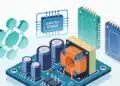
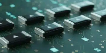
Power inductors are critical components in modern electronic systems, enabling energy storage, filtering, and voltage regulation across a wide range of applications. The relentless push toward higher efficiency, miniaturization, and reliability has driven significant innovation in inductor design. From early ferrite cores to advanced molded alloy powders and silicon-based inductors, the evolution reflects the industry’s response to rising switching frequencies, thermal challenges, and compact form factor requirements.
Key Takeaways
- Power inductors are essential in modern electronics for energy storage, filtering, and voltage regulation.
- The evolution of power inductors includes a shift from ferrite cores to advanced alloy powders, and now to silicon-based designs.
- Future trends focus on miniaturization, efficiency, and integration with innovations like polymer-bonded composites and AI-driven design.
- Silicon-based inductors offer ultra-thin profiles and cost-effective mass production, suitable for compact devices.
- The design process incorporates AI and digital twins, leading to faster development cycles and customized inductors for specific applications.
Chapter 1: Historical Evolution of Power Inductors
The earliest inductors were based on massive iron cores, offering high permeability and current handling but suffering from eddy current losses at higher frequencies. The 1970s–1980s marked the rise of ferrite-based inductors, which reduced AC losses and enabled switch-mode power supplies. However, ferrites introduced temperature-dependent saturation and leakage issues.
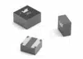
Chapter 2: Powdered and Molded Alloy Inductors
The 1990s–2000s saw the introduction of powdered iron and alloy-based inductors. By distributing air gaps throughout the core, these designs achieved stable saturation behavior and reduced eddy currents. Molded structures further improved space utilization and power density.
| Material | Advantages | Limitations |
|---|---|---|
| Ferrite | Low AC losses, good EMC performance | Temperature-dependent saturation, leakage fields |
| Powdered Iron | Stable saturation, distributed air gap, soft saturation | Lower permeability, larger size for high inductance |
| Alloy Powders | Improved efficiency, corrosion resistance, high current | Complex manufacturing, cost |
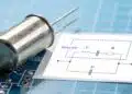
Chapter 3: State-of-the-Art Low-Loss Designs
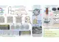
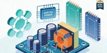
Recent innovations, such as Würth Elektronik’s WE-MXGI series, demonstrate ultra-low RDC and AC losses by combining nano-crystalline materials with optimized winding geometries. These inductors are particularly suited for GaN and SiC-based converters operating in the MHz range, where efficiency and thermal stability are paramount.
Chapter 4: Future Trends in Power Inductors
The future of power inductors is being shaped by three converging forces: miniaturization, efficiency, and integration. As switching frequencies in power electronics continue to rise—driven by GaN and SiC semiconductors—inductors must evolve to handle higher currents, lower losses, and increasingly compact footprints. Below we explore the most significant directions in which the technology is advancing.
4.1 Polymer-Bonded and Inorganic Composites
Traditional organic binders used in alloy powders are prone to degradation under high thermal and electrical stress, leading to the so-called percolation phenomenon. To counter this, researchers are developing polymer-bonded composites and even inorganic binders that offer:
- Improved thermal stability beyond 200 °C operating ranges.
- Resistance to long-term voltage stress and material breakdown.
- Potential for recyclability, aligning with circular economy goals.
By leveraging low-pressure polymer processing techniques (e.g., injection molding, extrusion), manufacturers can reduce internal cracking and enable the use of fragile, high-performance powders such as nano-crystalline alloys.
4.2 Clip-Based Inductors for Multiphase Systems
As CPUs, GPUs, and AI accelerators demand ever-higher currents, multiphase converters have become the norm. Clip-based inductors are emerging as the preferred solution for these systems, offering:
| Feature | Benefit | Applications |
|---|---|---|
| Dual-coil or multi-coil designs | Support for multiphase topologies with balanced current sharing | Server farms, AI accelerators, high-end GPUs |
| Powder-based clip cores | Soft saturation and stable inductance at high currents | Transient Load Voltage Regulation (TLVR) |
| Co-sintering processes | Combines molding and assembly for higher reliability | Next-gen CPU voltage regulators |
This transition from ferrite to powder-based clip inductors is critical for meeting the demands of MHz-range switching frequencies while maintaining efficiency and thermal stability.
4.3 Silicon-Based Inductors
Perhaps the most disruptive development is the rise of silicon-based inductors, fabricated using semiconductor processes. These wafer-level devices integrate copper windings and multilayer magnetic films directly on silicon substrates. Their advantages include:
- Ultra-thin profiles (as low as 200 µm), enabling direct PCB embedding.
- Wafer-level batch production, reducing cost per unit at scale.
- Flexible integration: solder-ball packaging, wire-bonding, or chiplet approaches.
Such inductors are already being demonstrated in 20 MHz switching converters with current ratings up to 400 mA, proving their viability for ultra-compact power modules in mobile devices, wearables, and IoT systems.
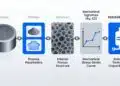
4.4 AI-Optimized Design and Digital Twins
Beyond materials, the design process itself is evolving. Companies are increasingly using AI-driven optimization and digital twin simulations to predict inductor performance under real-world conditions. This allows:
- Precise modeling of AC/DC losses across frequency ranges.
- Rapid iteration of winding geometries for minimal parasitics.
- Lifecycle prediction, including percolation and thermal fatigue effects.
The integration of AI into component design is expected to reduce development cycles and enable highly customized inductors for niche applications such as aerospace, EV drivetrains, and data center power delivery.
Conclusion
Power inductor technology has advanced from bulky iron cores to compact, high-efficiency, and application-specific designs. The future lies in integrating advanced materials, novel manufacturing processes, and semiconductor-level fabrication to meet the demands of high-frequency, high-current, and miniaturized systems. As electronics continue to evolve, inductors will remain a cornerstone of efficient power conversion.
Frequently Asked Questions (FAQ)
The main trends include polymer-bonded composites for higher thermal stability, clip-based inductors for multiphase systems, silicon-based wafer-level inductors, and AI-driven optimization for design and lifecycle prediction.
Silicon-based inductors enable ultra-thin profiles (as low as 200 µm), wafer-level batch production, and direct PCB embedding, making them ideal for mobile devices, IoT, and high-frequency converters.
They replace traditional organic binders with polymers or inorganic materials, reducing percolation effects, improving recyclability, and enhancing resistance to high temperature and voltage stress.
Key industries include automotive electrification, renewable energy, AI-driven data centers, and 5G/6G infrastructure, all of which demand compact, efficient, and reliable power inductors.
How-to: Optimize Power Inductor Selection for High-Frequency Applications
- Define Application Requirements
Identify switching frequency, current rating, and thermal constraints. For GaN/SiC converters, prioritize MHz-range compatibility.
- Choose Core Material
Select between ferrite, alloy powder, or nano-crystalline composites. For high-frequency, low-loss applications, nano-crystalline or polymer-bonded composites are recommended.
- Evaluate Inductor Geometry
Consider winding type (round wire vs. flat wire), clip-based structures for multiphase systems, or silicon-based wafer inductors for ultra-compact designs.
- Simulate and Optimize
Use AI-driven digital twin simulations to predict AC/DC losses, thermal behavior, and lifecycle performance before final selection.
- Validate in Real Conditions
Test inductors under expected load, temperature, and transient conditions to ensure compliance with efficiency and reliability targets.