






An X2Y bypass capacitor is a four-terminal, three-node capacitor with an internal shielding electrode arrangement designed to reduce inductance and provide closely matched capacitive paths.
This article explains its construction, bypass and EMI-filtering connections, comparison with conventional MLCC networks, and practical selection and PCB-layout checks for design and component engineers.
The original article was based on material from Knowles Precision Devices and a comparison attributed to X2Y Attenuators, LLC. X2Y technology was developed by X2Y Attenuators; the discussion below separates the operating principle from application-dependent performance and component-count claims. [1]
Key Takeaways
- An X2Y component has two line electrodes and a shared shielding electrode brought out through two ground terminations: four terminals, but three electrical nodes.
- Its low-inductance construction can support broadband bypassing and balanced EMI filtering, but the mounted result depends strongly on PCB connections.
- For single-rail bypassing, the two capacitor sections can be connected in parallel. For balanced filtering, each line connects to a separate section and both ground terminals connect to the intended reference.
- Closely matched sections reduce imbalance; they do not eliminate the dielectric’s temperature dependence, DC-bias dependence or aging.
- X2Y is not an X2 or Y2 safety classification. Mains and insulation-barrier applications require the appropriate safety-approved component and insulation design.
X2Y Bypass Capacitor Construction and Operating Principle
X2Y technology uses a special electrode arrangement within a multilayer component. In ceramic implementations, it uses familiar MLCC manufacturing materials and processes, but changes the internal electrode geometry and external connections. [1, 2]
Four terminals, three electrical nodes
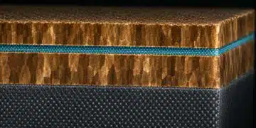
A conventional two-terminal MLCC contains opposing electrode sets separated by dielectric layers. An X2Y construction adds shielding electrodes around the line electrodes, producing two closely matched line-to-reference capacitor sections within one package. The line terminals are commonly identified as A and B, and the shielding electrode is accessible through G1 and G2. These two ground terminations belong to the same electrical node. [1, 2]

The internal geometry reduces effective series inductance through closely coupled current paths and opposing magnetic fields. This can extend the useful low-impedance response compared with a conventional arrangement, but the component does not have zero inductance. Pads, vias, traces and the reference connection contribute to its installed impedance. [2, 3]
Capacitance depends on the connection
Check whether the datasheet capacitance describes one line-to-ground section or the complete bypass connection. In Johanson’s documented convention, the catalog value refers to one section between A or B and ground. Connecting A and B together places the two sections in parallel, giving twice the nominal per-section capacitance under the same measurement conditions. This connection does not double the voltage rating. [2]
Do not assume that a value quoted for one section is the capacitance measured directly between A and B. Use the selected manufacturer’s equivalent circuit, terminal definitions and measurement conditions when comparing parts or simulation models.
Using X2Y for Bypass, Decoupling, and EMI Filtering Components
The same internal structure supports several circuit connections. The correct choice depends on whether the objective is supply bypassing, filtering a balanced pair, or decoupling two supply rails. The component’s terminal count alone does not identify the required connection. [2, 3]
Single-rail supply bypassing
For the documented parallel-section bypass connection, connect A and B to the same supply rail and connect G1 and G2 to its local return. Both sections then support the same rail. Their low-inductance connection can provide a useful alternative to a network of conventional MLCCs where mounted inductance is a limiting factor. [2]
A reduction in component count is possible, not automatic. Check the effective capacitance, installed impedance and transient response of the complete power-distribution network. A specialist local bypass capacitor does not automatically replace bulk storage or override the IC and regulator manufacturers’ capacitor requirements.
Balanced-line and dual-rail filtering
For a balanced pair, connect one line to A and the other to B, with G1 and G2 connected through low-inductance paths to the intended reference. Common-mode noise has a capacitive path from each line to that reference, while the network also provides differential-mode attenuation. Closely matched paths help limit conversion of common-mode interference into differential error. [2, 3]
Possible applications include amplifier inputs, suitable twisted-pair interfaces and motor-terminal suppression. Each requires a suitable capacitance and reference connection. A capacitor that attenuates unwanted interference also loads the wanted signal, so verify signal bandwidth, source impedance and the interface requirements rather than treating X2Y as a universal high-speed data-line filter.
In a dual-rail amplifier application, A and B can serve different supply rails while the shielding node connects to their common reference. This is different from tying A and B together for single-rail bypassing. Check the selected component’s permitted terminal voltages and the amplifier’s recommended decoupling arrangement. [2, 3]
Bypass operation is not feedthrough operation
An X2Y component used as a shunt filter does not carry the load’s steady DC current through a series path inside the component. This distinguishes it from a feedthrough filter whose through-path must carry load current. Consequently, the bypass connection adds no series DC resistance to the load conductor. [3]
This does not mean unlimited electrical capability. The component still carries AC filtering or transient current and remains subject to voltage, dielectric-loss, heating and connection limits. Evaluate these limits for the actual waveform. Small-signal input filtering and power-converter decoupling impose different current and energy demands.
Matched sections are not invariant capacitors
The two sections share a construction and thermal environment, which improves tracking compared with independently selected parts. However, their absolute capacitance still follows the selected dielectric’s characteristics. Class 2 ceramic implementations require assessment of DC bias, temperature and aging; the X2Y electrode arrangement does not remove these material effects. [1, 2]
For balanced filtering, also consider whether the two sections operate at different DC voltages. Close matching under a common test condition is not sufficient evidence of equal capacitance under unequal operating bias. Use the supplier’s matching information and operating-condition data when imbalance affects the error budget.
Comparing Conventional MLCC Configurations to an X2Y Design
The original article illustrated an amplifier-decoupling comparison attributed to X2Y Attenuators, LLC. One arrangement used a single X2Y component for both amplifier power pins; the conventional arrangement used two capacitor values per power pin, giving four MLCCs in total.


The original account states that ground attachment and capacitor setbacks were matched and that parasitics were equalized between the arrangements. These are important comparison objectives: changes in connection geometry can otherwise dominate the measured difference.
The component-count comparison demonstrates an integration opportunity, not a universal substitution rule. A valid engineering comparison must establish the effective capacitance of each connection, the mounted impedance, supply conditions, amplifier operating point, noise measurement location and measurement bandwidth.
Replacing several capacitors with one package can reduce placements and routing demands. Whether it reduces total board area, mass or cost depends on the selected packages, land patterns, vias, unit prices and qualification effort. Compare the complete implementation rather than the number of capacitor symbols alone.
PCB Layout and Measurement
Low component inductance is useful only when the board preserves a low-inductance current path. The manufacturer’s layout guide emphasizes connecting both ground terminals and locating the filter according to the interference path. [3]
Connect both ground terminals
- Connect both G1 and G2 to the intended reference using short, low-inductance paths.
- Use the selected part’s land pattern and review the complete supply or signal return path, including vias and reference-plane access.
- For sensitive-input immunity, place the filter near the protected input. For cable-related emissions, consider the PCB entry or exit point.
- Where a shielded enclosure is part of the filtering strategy, keep the connection to the relevant enclosure or bulkhead reference low in inductance.
- Avoid long flying-wire evaluations: their inductance can obscure the component’s intended high-frequency behavior. [3]
Validate the installed network
Compare candidate networks under the same operating conditions and measurement setup. For supply decoupling, check load-related voltage excursions and noise at the relevant device connections. For input filtering, check wanted-signal response as well as interference rejection.
A single low-inductance component can avoid some interactions between discrete capacitor branches, but it does not eliminate resonances elsewhere in the board or power-distribution network. Include surrounding capacitors and interconnects when assessing impedance peaks. Manufacturer component comparisons should not be interpreted as guarantees for every PCB. [2]
Use the manufacturer’s assembly guidance. Four-terminal ceramic parts remain susceptible to thermal and mechanical cracking, and a damaged prototype can produce misleading filtering results. Follow the current soldering instructions for the selected part rather than applying a generic hand-soldering process. [3]
Design and Selection Checklist
Start with the required circuit function and operating conditions, then select the component and mounting arrangement together. A catalog X2Y part is a candidate for a defined requirement, not an automatically superior replacement for a conventional MLCC network.
Electrical and datasheet checks
- Define the function: single-rail bypassing, dual-rail decoupling, balanced input filtering or motor-terminal suppression.
- Confirm A, B, G1 and G2 assignments, the equivalent circuit and whether nominal capacitance refers to one section or the connected combination.
- Compare effective capacitance at operating bias and temperature, including tolerance and relevant aging information.
- Check working voltage and expected transients using the manufacturer’s terminal-voltage definitions and derating guidance.
- Compare impedance, equivalent series resistance and equivalent series inductance over the relevant band, including mounting effects.
- For balanced inputs, check section matching, unequal bias conditions and wanted-signal loading. For supply use, check transient-current capability, heating and compatibility with the complete supply network. [2, 3]
Catalog parts, custom requirements and qualification
For catalog parts, record the complete manufacturer part number, dielectric, voltage rating, capacitance convention, tolerance, termination and footprint. Qualify alternatives against the same installed electrical requirements rather than accepting nominal capacitance and package size as proof of interchangeability.
If a custom construction is necessary, specify terminal connections, operating voltages, capacitance and matching requirements, mounted impedance objectives, mechanical constraints and acceptance tests. Confirm the required environmental qualification, screening, traceability and production-change controls for the actual application.
Safety and application boundaries
X2Y is a technology name, not an X2, Y2 or combined safety approval. Likewise, the use of X and Y to describe equivalent-circuit branches does not establish a component’s suitability for connection to mains or across an insulation barrier. Safety capacitor datasheets identify their applicable classifications and approvals explicitly. [1, 4]
For a safety-related connection, select a component with the required approval and verify the equipment’s insulation, clearance, creepage and leakage-current requirements. A high DC voltage rating alone does not establish safety suitability. Keep ordinary low-voltage signal filtering separate from mains suppression and power-stage energy-storage requirements.
Conclusion
X2Y components combine a shielding-electrode arrangement, closely matched capacitor sections and multiple external connections to support low-inductance bypassing and balanced EMI filtering. Their benefit depends on using the correct circuit connection and preserving short, low-inductance paths on the PCB.
Select by effective capacitance, terminal voltage, dielectric behavior, installed impedance and application requirements. Validate the complete circuit before reducing component count, and treat safety approval, qualification and production interchangeability as separate checks.
FAQ
An X2Y bypass capacitor uses shielding electrodes and two closely matched capacitor sections in a four-terminal package. It has three electrical nodes because its two ground terminations connect to a shared shielding node. The arrangement supports low-inductance supply bypassing and balanced EMI filtering when the terminal connections and PCB layout suit the application.
For the documented single-rail parallel connection, connect A and B to the same supply rail and connect both ground terminals to the local return through low-inductance paths. Check the manufacturer’s capacitance convention: paralleling the two sections doubles their per-section nominal capacitance under matching measurement conditions, but does not double the voltage rating.
It can replace several parts when its connected capacitance and installed impedance meet the same circuit requirements. Replacement is not determined by component count alone. Compare operating bias, temperature, transient response, signal loading where relevant and PCB geometry. Retain bulk capacitance or other network elements when the load, regulator or filtering requirement still needs them.
No. The integrated sections can track closely because they share a construction and environment, but their absolute capacitance still follows the dielectric’s characteristics. Class 2 ceramic versions require checks for DC bias, temperature and aging. Unequal voltages on the two sections also require attention when capacitance balance affects the circuit’s error budget.
No. X2Y identifies an electrode technology, not a safety classification. A part intended for mains suppression or an insulation-barrier connection needs the appropriate explicit safety approval and must satisfy the equipment’s insulation requirements. Neither the technology name nor a sufficiently high DC voltage rating establishes that approval or makes an ordinary part interchangeable with a safety capacitor.
How to Select and Validate an X2Y Capacitor
Select an X2Y capacitor and validate its connection, PCB mounting and circuit performance before approving the production implementation.
- Define the circuit requirement
Identify single-rail bypassing, dual-rail decoupling or balanced-line filtering. Record operating voltages, the wanted signal band or load behavior, the interference path and the permitted disturbance.
- Check connections and operating data
Confirm terminal assignments, the equivalent circuit and the capacitance convention. Compare effective capacitance, matching, voltage limits, dielectric behavior and impedance under the intended operating conditions.
- Design the low-inductance mounting
Use the selected part’s land pattern and connect both ground terminals to the intended reference. Keep the complete current paths short and locate the component according to the protected input, supply connection or cable interference path.
- Compare and measure the complete circuit
Evaluate the candidate and conventional networks under matching conditions. Check supply transients or wanted-signal response as appropriate, measure interference rejection and investigate resonances or unexpected heating before reducing component count.
- Release the qualified implementation
Confirm assembly instructions, environmental qualification and any required safety approvals. Record the approved part number, footprint, operating data and acceptance tests, and reassess alternatives that change capacitance, matching or installed impedance.
Further Reading
These background articles expand the capacitor, layout and filtering principles used in X2Y applications.
- Introduction to EMI Filtering: interference paths, filter placement and terminology.
- Bypass Capacitor: local current paths, mounting inductance and supply-network validation.
- Coupling and Decoupling Capacitors: effective capacitance, network interactions and practical selection.
- MLCC and Ceramic Capacitors: ceramic dielectric classes, construction and operating limitations.
References
The following technical documents support the construction, connection, layout and safety distinctions cited in the article. Use the current datasheet for the selected production part.
- X2Y Attenuators, Technology Summary, X2Y Attenuators, undated; accessed November 5, 2026.
- Johanson Dielectrics, X2Y Filter and Decoupling Capacitors, publication X2Y0210, Johanson Dielectrics, 2010.
- Steve Cole, X2Y EMI Filter Evaluation and PCB Design Guidelines, Johanson Dielectrics, 2009.
- Johanson Dielectrics, AC Safety, SMT – UL and TUV Certified Capacitors, Johanson Dielectrics, undated; accessed November 5, 2026.
Latest technical review and revision: November 5, 2026. Updated terminal connections, capacitance interpretation, dielectric limitations, PCB guidance, selection and safety checks; retained the original three figures and amplifier-comparison context.