


Prof. Sam Ben-Yaakov in this video explains how to calculate the resistor value of an RC snubber (RCD clamp) in flyback converter.
Key Takeaways
- RC snubbers limit voltage spikes caused by leakage inductance during switch turn-off.
- Clamp voltage must exceed reflected voltage to avoid continuous current through the snubber.
- A compact formula relates snubber resistance to clamp voltage, reflected voltage, leakage energy, and switching frequency.
- Designers balance resistor values to manage voltage, reduce losses, and ensure reliable converter operation.
Introduction
This article based on prof. Sam Ben-Yaakov video explains how to calculate the resistor value of an RC snubber (RCD clamp) used across the primary switch of a flyback converter. The discussion follows a simulated flyback converter example to highlight the role of leakage inductance and snubber design in limiting overvoltage on the switch.
The focus is on deriving a practical expression for the snubber resistor value based on the leakage inductance energy and the chosen clamp voltage, while clarifying a common misunderstanding: that the snubber power is determined only by the leakage inductance energy.
Key points
- A flyback converter’s leakage inductance causes a high voltage spike on the primary switch at turn‑off.
- An RC snubber (RCD clamp) limits this spike by clamping the drain voltage to a defined level.
- The clamp voltage is the sum of the input voltage and the snubber capacitor DC voltage.
- The capacitor is chosen so its ripple is small, so it can be treated as a near‑constant voltage source.
- The reflected output voltage from secondary to primary must be considered when selecting the clamp voltage.
- The clamp voltage must be higher than the reflected voltage to avoid continuous current flow through the snubber diode.
- The average current through the snubber resistor equals the average current through the equivalent clamp voltage source (no average current through the capacitor).
- The power dissipated in the snubber resistor includes contributions from both the leakage inductance and the input source.
- A compact formula can be derived for the snubber resistance in terms of clamp voltage, reflected voltage, leakage inductance energy and switching frequency.
- Increasing leakage energy requires lowering the snubber resistance to maintain the same clamp voltage; increasing clamp voltage allows a larger snubber resistance.
Flyback RC Snubber Principles and Resistance Value Calculation
In a flyback converter, the primary winding is magnetizing the core during the on‑time of the switch, while the secondary is effectively disconnected because its rectifier diode is reverse‑biased. When the switch turns off, the primary current is suddenly interrupted, and the energy stored in both the magnetizing inductance and the leakage inductance must be transferred elsewhere. The magnetizing energy ideally transfers to the secondary and then to the load. However, the leakage inductance is not coupled to the secondary; its energy appears as a voltage spike at the primary switch node, which can exceed the device’s voltage rating and cause failure.
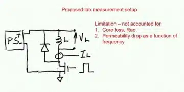
To prevent the switch overvoltage, an RC snubber (often implemented as an RCD clamp) is connected from the switch node to the input rail through a diode. In the example, the flyback operates at around 100 kHz and 0.4 duty cycle, with 30 V input and a 1 µH leakage inductance referred to the primary. Without a snubber, the simulated drain‑source voltage of a 100 V MOSFET reaches approximately 150 V at turn‑off, clearly beyond the device rating. With the snubber connected, the drain voltage is clamped to about 55 V, well within a safe margin for the transistor.
The clamp voltage observed at the switch node can be decomposed into two contributions: the input voltage Vin and the voltage on the snubber capacitor. In the numerical example, the input voltage is 30 V and the measured clamp level is about 55 V, implying that the snubber capacitor is charged to roughly 25 V in steady state. The capacitor is chosen so that its voltage ripple over a switching period is small, which allows it to be modeled as a near‑constant voltage source. Together with the input supply, it forms an effective clamp voltage source that defines the maximum switch voltage at turn‑off.
Simultaneously, the reflected output voltage must be considered. The transformer’s secondary inductance is one quarter of the primary inductance, which implies a turns ratio such that the primary voltage is approximately twice the output voltage in flyback operation. With a 10 V output, the reflected voltage to the primary is therefore about 20 V. The clamp voltage on the snubber capacitor (about 25 V) exceeds the reflected voltage only by 5 V, which is a small margin. This is operational but not ideal; for robust design, one typically chooses a higher clamp level to provide more overhead above the reflected voltage.
At the instant of switch turn‑off, the primary current has a peak value determined by the load and operating conditions. As the switch opens, the reflected secondary voltage appears across the primary, and the current through the leakage inductance is diverted through the snubber diode into the RC network. The current then decays to zero while energy is transferred first to the clamp capacitor (updating its voltage) and ultimately dissipated as heat in the snubber resistor. During the rest of the off‑time, the magnetizing energy flows through the transformer secondary into the output, while the primary current is essentially zero except for small parasitic oscillations.
A common but incorrect approach is to assume that the entire additional power handled by the snubber is simply the energy stored in the leakage inductance, given bymultiplied by the switching frequency. This ignores that the primary current during the leakage‑related transient flows while a non‑zero voltage is applied across the primary, so the power balance must account for both the leakage energy and the interaction with the clamp voltage. The video provides a more accurate method by using average currents and voltages.
The key observation is that over one full switching period there is no net average current through the snubber capacitor, because its voltage returns to nearly the same value each cycle. As a result, the average current through the snubber resistor must equal the average current through the equivalent clamp voltage source (the input supply plus the capacitor voltage) over the same period. This allows one to relate the resistor current, the clamp voltage and the energy coming from the leakage inductance.
The average current through the snubber resistor is simply the clamp voltage divided by the resistance , assuming that the resistor sees an almost constant voltage equal to in steady state:Because of charge balance on the capacitor, this is also the average current leaving the equivalent voltage source (input plus capacitor). The total average power dissipated in the resistor, , must then equal the sum of the power delivered by the leakage inductance, , and the power delivered by the input source during the clamp interval:By expressing these power terms in terms of leakage energy, clamp voltage and reflected voltage, one can derive a compact design expression for the snubber resistance. The result has the general structurewhere is the reflected secondary voltage to the primary and is the switching frequency. Here, the numerator represents the product of the clamp voltage and the voltage difference between the clamp and the reflected voltage, while the denominator scales with the leakage energy per cycle and the switching frequency (hence the power content). This form captures the correct dependence on both the leakage energy and the voltage levels involved.
An important practical condition emerges from this expression: the clamp voltage must be larger than the reflected voltage, . If this were not the case, the term would become negative, implying a negative resistance in the formula, which is non‑physical. In circuit terms, if the reflected voltage exceeded the clamp voltage, there would be a continuous current through the snubber path even after the leakage‑related transient, because the primary voltage driven by the reflected secondary would be higher than the clamp capacitor voltage. To avoid this, the clamp voltage must be chosen sufficiently above the reflected voltage, ensuring that the snubber only conducts during the intended transient interval.
The design consequences are clear. For a given clamp voltage and reflected voltage, increasing the leakage inductance energy (for example, due to higher leakage inductance or higher primary peak current) requires a lower snubber resistance to absorb more energy and maintain the same clamp level. Conversely, choosing a higher clamp voltage allows the use of a larger resistor, which reduces snubber current and losses but increases stress on the switch. Designers therefore balance switch voltage margin, snubber power dissipation and transformer design to arrive at an appropriate clamp voltage and corresponding resistor value.
Conclusion
After working through this approach, the reader should be able to size the resistor in a flyback RC snubber (RCD clamp) using a physically consistent energy and average‑current argument, rather than relying on the leakage inductance energy alone. The derived relation ties the resistor value to the clamp voltage, reflected secondary voltage, leakage energy and switching frequency, and highlights the requirement that the clamp voltage exceed the reflected voltage. In practice, this method supports robust flyback converter design by ensuring safe switch voltage, controlled snubber losses and proper handling of leakage energy.
Flyback RC snubber design – FAQ
An RC snubber (often implemented as an RCD clamp) limits the voltage spike at the primary switch node caused by leakage inductance when the MOSFET turns off. By clamping the drain voltage to a defined level, it protects the switch from exceeding its maximum voltage rating and improves reliability.
Leakage inductance is not magnetically coupled to the secondary winding, so its stored energy cannot transfer to the load when the switch turns off. Instead, this energy forces the switch node voltage to rise rapidly, producing a high transient spike that can exceed the MOSFET’s voltage rating.
The clamp voltage seen at the MOSFET drain is the sum of the input voltage and the DC voltage on the snubber capacitor. The transformer also reflects the output voltage to the primary, so the clamp level must be chosen with respect to both the input voltage and the reflected secondary voltage.
If the clamp voltage is not higher than the reflected output voltage, current will continue to flow through the snubber path even after the leakage energy is removed. This causes unnecessary continuous dissipation and contradicts the design assumption that the snubber only conducts during the transient clamp interval.
A frequent mistake is to assume that snubber power equals only the energy stored in the leakage inductance multiplied by the switching frequency. This ignores the fact that the leakage current flows while a nonzero voltage appears across the primary, so power also depends on the clamp voltage and reflected voltage.
Over a switching period, the snubber capacitor’s voltage returns approximately to the same value, so its net average current is zero. Therefore, the average current through the snubber resistor equals the average current through the equivalent clamp voltage source and can be expressed as the clamp voltage divided by the snubber resistance.
The snubber resistance depends on the clamp voltage, the reflected output voltage, the leakage inductance energy at peak current, and the switching frequency. Higher leakage energy requires a lower resistance to maintain the same clamp level, while a higher clamp voltage allows a larger resistance but increases switch stress.
How to calculate the resistance value of a flyback RC snubber
- Step 1: Gather key flyback converter parameters
Collect the essential design data from your flyback converter. You need the input voltage Vin, the output voltage, the transformer turns ratio (or primary and secondary inductances), the leakage inductance referred to the primary Llk, the peak primary current Ipk, and the switching frequency fs. These parameters determine the reflected voltage and the leakage energy that the snubber must handle.
- Step 2: Compute the reflected output voltage to the primary
Use the transformer turns ratio to calculate the voltage reflected from secondary to primary. If the turns ratio and output voltage are known, compute the reflected voltage as , where n is the appropriate primary-to-secondary ratio. This reflected voltage appears on the primary during the off-time when the secondary delivers energy to the load.
- Step 3: Choose a suitable clamp voltage level
Select a clamp voltage Vclamp that keeps the MOSFET drain-source voltage within its safe operating limits while providing some margin above the reflected voltage. The clamp voltage is the sum of the input voltage and the snubber capacitor’s DC voltage. Ensure that Vclamp is significantly higher than Vref but still comfortably below the MOSFET’s maximum rating, including layout parasitics and tolerances.
- Step 4: Estimate the leakage inductance energy per switching cycle
Calculate the energy stored in the leakage inductance at the moment of switch turn-off. This energy is given by . Multiply this energy by the switching frequency fs to understand the power contribution from the leakage inductance, which the snubber network must dissipate together with the contribution from the clamp voltage source.
- Step 5: Use the snubber resistance formula including clamp and reflected voltages
Apply the relationship that ties the snubber resistance to clamp and reflected voltages, leakage energy, and switching frequency. The resistance can be expressed in the form . This captures the average power balance between the leakage inductance and the clamp voltage source, ensuring that the snubber resistor dissipates the correct amount of energy per cycle.
- Step 6: Verify that the clamp voltage is higher than the reflected voltage
Check that Vclamp > Vref. If this condition is not met, the formula would yield a nonphysical resistance and, in practice, current would continue to flow through the snubber even after the transient, causing continuous power loss. Adjust the clamp voltage target or transformer design until this condition is safely satisfied before finalizing the resistor value.
- Step 7: Choose a practical resistor and validate in simulation or hardware
Select the nearest standard resistor value with adequate power rating and voltage capability based on the calculated resistance and expected dissipation. Verify performance using circuit simulation or bench measurements, checking that the MOSFET drain voltage is properly clamped, the snubber does not conduct continuously, and the resistor temperature remains within safe limits under worst-case operating conditions.
References
- Sam Ben‑Yaakov, “Calculating the resistance value of a Flyback RC snubber (corrected),” YouTube video, https://www.youtube.com/watch?v=mUw7iuUmrHA