


Crystal units are often modeled as “black boxes” in schematics, but their internal equivalent circuit strongly influences oscillation frequency, stability and start‑up behavior.
Key Takeaways
- Crystal units behave as resonant RLC networks. A crystal unit is modeled by a motional branch in series, in parallel with a shunt capacitance , so it behaves like a high‑Q resonant network rather than a simple capacitor.
- Equivalent constants directly affect stability and start‑up. Motional inductance , motional capacitance , motional resistance and shunt capacitance determine resonance frequencies, frequency pulling, effective resistance and quality factor Q, which in turn set stability, phase noise and start‑up margin.
- Load capacitance shifts frequency and impedance. The oscillation frequency and load resonance resistance change with load capacitance ; smaller increases frequency deviation and effective resistance, so matching to the crystal specification is critical.
- Equations enable accurate design‑in. Closed‑form equations for , , , , and Q let engineers predict how a crystal will behave with a given load network and back‑calculate actual from a measured oscillation frequency.
- Circuit matching services reduce risk. Manufacturer circuit matching support evaluates the crystal and oscillator IC together, optimizing load capacitance and component values to ensure reliable start‑up, sufficient gain margin and stable oscillation in production designs.
Introduction
Crystal units are fundamental building blocks of timing circuits, but their behavior is far from that of an ideal capacitor or inductor. Their electrical performance is best understood through an equivalent circuit with well‑defined constants, which directly impact oscillation frequency, stability, start‑up margin and tuning range. This white paper summarizes the Kyocera model of crystal unit equivalent circuit constants and translates it into practical guidance for design engineers working on reference oscillators.
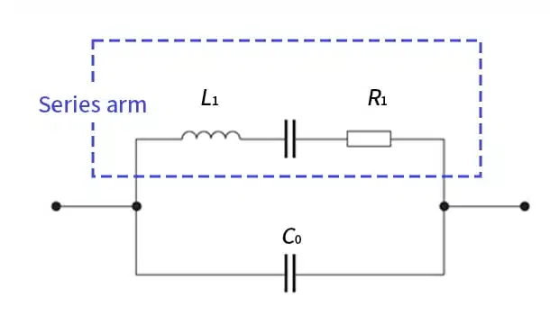
Equivalent circuit model of a crystal unit
The vibration (mechanical resonance) of a crystal element is modeled by an electrical equivalent circuit consisting of a motional branch in series and a shunt capacitance in parallel. The motional branch represents the elastic and inertial properties of the vibrating crystal, while the shunt element represents the static electrode capacitance.
Standard equivalent circuit
The commonly used one‑port equivalent circuit of a crystal unit is:
- Motional inductance
- Motional capacitance
- Motional resistance
- Shunt (static) capacitance
The motional elements , and are connected in series, and this series branch is placed in parallel with the shunt capacitance .
Physical meaning of each constant
Motional inductance L1
- Represents the inertial component of the vibrating crystal in the series arm.
- A larger corresponds to a higher quality factor Q and increased oscillation stability.
- High Q implies a narrower resonance, which is beneficial for low phase noise and jitter in clock and RF applications.
Motional capacitance C1
- Represents the elastic (spring‑like) component of the crystal resonance.
- A larger leads to a larger frequency variation with respect to changes in load capacitance.
- For high stability oscillators, is typically designed small to reduce sensitivity to parasitic and tolerance variations in the load network.
- For VCXOs and other tunable oscillators, a larger is desirable to realize a wider frequency pulling range with practical tuning capacitances.
Motional resistance R1
- Represents the loss resistance of the vibrating crystal in the series branch, corresponding to the resistance at which conductance is maximized in the admittance circle diagram.
- A smaller is generally preferable, as it indicates lower loss and makes oscillation start‑up easier with higher gain margin.
- Excessively high may cause start‑up failures or marginal oscillation, especially at low supply voltages or extreme temperatures.
Shunt capacitance C0
- Represents the static capacitance between the electrodes of the crystal unit.
- Determined primarily by electrode thickness, electrode area, and package geometry.
- The equivalent constants are influenced by electrode design; generally, the smaller the crystal unit and its electrode area, the smaller .
- and are inversely proportional; as one increases, the other decreases in designs with similar frequency targets.
Fundamental equations from equivalent constants
Here are a set of core equations that relate the equivalent circuit constants to the resonance frequencies, effective resistance, load capacitance and quality factor of a crystal unit.
Series and parallel resonance
The series resonance frequency is determined only by the motional inductance and motional capacitance:The parallel resonance frequency is determined by the motional elements and the shunt capacitance:The capacity ratio γ expressing the ratio between shunt and motional capacitance, is:A higher capacity ratio implies a larger separation between series and parallel resonance frequencies and stronger influence of stray capacitances.
Load resonant frequency
When a load capacitance is connected in the oscillator circuit, the oscillation frequency shifts from the series resonance. The load resonant frequency is expressed by:
Design implications:
- As changes, moves away from ; smaller increases the magnitude of the frequency shift.
- The term quantifies how strongly the load capacitance pulls the frequency; a larger or smaller denominator results in stronger pulling.
- For tight‑tolerance clocks, both and the effective should be controlled carefully to keep this term small.
Load resonance resistance
The effective load resonance resistance of the crystal unit when a load capacitance is connected is:Here:
- As decreases, the factor increases, so rises and loop gain decreases.
- For a given oscillator IC with limited transconductance, too large an can cause poor start‑up margin or outright failure to oscillate.
- When is chosen close to the datasheet recommendation, remains in the intended range, ensuring robust operation.
Load capacitance from measured oscillation frequency
Direct expression for calculating the effective load capacitance can be derived from a measured oscillation frequency and the series resonance frequency :This equation is particularly useful in lab evaluation:
- The designer measures on the assembled PCB and uses known , and from the datasheet to back‑calculate the actual .
- The inferred can be compared to the schematic value to estimate the contribution of stray capacitance and component tolerances.
- If necessary, external capacitors or trimmers can be adjusted to bring and thus into the desired range.
Quality factor Q
The quality factor Q of the crystal’s motional branch is defined in two equivalent ways:In practice:
- Higher Q indicates lower energy loss per cycle and a narrower resonance bandwidth, which improves phase noise performance.
- For a given , increasing or decreasing raises Q; this is typical for high‑frequency, small‑C1 crystal designs.
- Oscillator circuitry must provide sufficient loop gain while respecting the maximum drive level, as high‑Q crystals can be more sensitive to over‑drive and non‑linearities.
Equation summary table
| Quantity | Equation |
|---|---|
| Series resonance | |
| Parallel resonance | |
| Capacity ratio | |
| Load resonant | |
| Load resistance | |
| Load capacitance | |
| Quality factor Q |
Frequency and impedance versus load capacitance
In a practical oscillator circuit, the crystal is connected with an effective load capacitance that includes both external load capacitors and stray capacitances from the IC and PCB. The equivalent circuit constants interact with to determine the oscillation frequency and impedance seen by the oscillator.
Frequency behavior with load capacitance
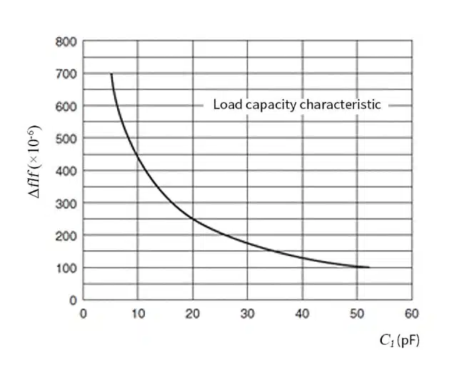
The formula for shows that the frequency changes when the load capacitance connected to the crystal unit is changed. The smaller the , the greater the change in frequency relative to the datasheet nominal value. The slope of the load capacitance characteristic varies depending on the frequency, shape and overtone order of the crystal unit, so different devices exhibit different pulling behavior for the same change in .
In practice, designers use trimmer capacitors or adjustable component values in the oscillator network to fine‑tune and trim the output frequency to the target value, using the equations and constants from the datasheet as a guide.
Impedance behavior with load capacitance
The formula for shows the change in impedance when a load capacitance is connected. As decreases, the impedance of the crystal unit increases. This affects the loop gain of the oscillator and can lead to marginal or unstable operation if becomes too large for the available transconductance of the oscillator IC.
A qualitative view is summarized in the table below.
| Load capacitance | Frequency (vs. target) | Effective resistance | Design note |
|---|---|---|---|
| Very small | Larger deviation from nominal | Highest | Risk of marginal start‑up, strong pulling |
| Nominal (datasheet value) | At specified nominal frequency | Nominal | Recommended operating point |
| Larger than nominal | Frequency closer to series value | Lower than at very small | Reduced pulling range, may ease start‑up |
Using oscillation frequency to infer load capacitance
As mentioned previously, the series resonance frequency of a crystal unit changes in accordance with the load capacitance of the oscillation circuit. In practical oscillation circuits, the load capacitance is adjusted using components such as trimmer capacitors to fine‑tune the oscillation frequency.
With explicit formula for , the designer can:
- Measure in the assembled circuit under nominal conditions.
- Use the known , and from the datasheet to compute the effective .
- Compare the result to the intended schematic value to estimate stray contributions and tolerance accumulation.
- Adjust component values or layout guidelines based on this insight for future revisions.
Practical implications for crystal selection
Looking beyond nominal frequency and load capacitance to the full set of equivalent circuit constants can significantly improve first‑pass success.
Design implications of each constant
- A smaller improves start‑up reliability, especially in low‑power or low‑supply‑voltage oscillators.
- The ratio between and the specified determines how sensitive frequency will be to load variations and parasitics.
- affects how much the actual parallel resonance deviates from the ideal series resonance and can influence EMC behavior and coupling into nearby high‑impedance nodes.
- Because and are inversely related for a given resonance, compact high‑frequency units typically have small and large , which can increase Q but also sensitivity to circuit conditions.
- For VCXOs and other tunable oscillators, choosing a crystal with appropriate is essential to achieving the desired tuning range without excessive control voltage or non‑linear behavior.
Recommended checklist for engineers
When designing‑in a crystal unit:
- Always use the manufacturer’s datasheet values for , , and when simulating oscillator start‑up and margin.
- Dimension the external capacitors so that the total load capacitance, including IC and PCB contributions, matches the specified of the crystal.
- Check that the effective resonance resistance for your chosen lies within the oscillator IC’s recommended range.
- Respect the specified maximum drive level, particularly for high‑Q, low‑loss crystals.
- For high‑stability or wide‑range tuning applications, use the frequency‑versus‑load relationship to estimate how much frequency shift you get per picofarad of load change and size trimmer ranges accordingly.
Circuit matching support
To ensure customers can use timing devices with peace of mind, leading manufacturers offers technical support centers to provide circuit matching services. In this service, the crystal unit and the oscillator IC are evaluated together, and the load capacitance and associated network are optimized for higher gain margin, more stable oscillation and improved start‑up time.
For complex high‑frequency designs, automotive timing circuits or very tight frequency‑stability requirements, engaging such a matching service can significantly reduce design iterations and production risk.
Conclusion
By modeling crystal units with the equivalent circuit constants , , and , engineers gain a clear handle on how resonance frequencies, load capacitance and quality factor shape real oscillator behavior. Using the manufacturer’s equations for , , , and Q makes it possible to predict frequency pulling, verify start‑up margin and optimize load networks before hardware tuning. Combined with circuit matching support from manufacturers, these tools help reduce design iterations and deliver stable, low‑jitter timing solutions that meet demanding specifications in modern electronic systems.
FAQ
The main constants are motional inductance , motional capacitance , motional resistance , and shunt capacitance ; together they form the standard RLC model of a crystal unit and define its resonant behavior.
The series resonance frequency depends only on and , while the parallel resonance frequency depends on , and , so is slightly higher than and more sensitive to shunt and stray capacitances.
When a load capacitance is connected, the crystal operates at a load resonant frequency derived from , , and ; changing alters the effective reactance seen by the motional branch and shifts the oscillation frequency.
By measuring the oscillation frequency on the assembled board and using the manufacturer’s equation relating ,, and , you can back‑calculate the effective and compare it with your schematic load capacitance.
Lower means lower loss and a smaller effective load resistance , so the oscillator IC needs less transconductance to satisfy the Barkhausen criterion and the circuit starts up more reliably across temperature and voltage.
How to use crystal equivalent circuit constants in oscillator design
- Collect the crystal datasheet parameters
Gather the specified series resonance frequency , motional inductance , motional capacitance , motional resistance , shunt capacitance , recommended load capacitance and maximum drive level.
- Choose an oscillator IC and topology
Select an oscillator IC that supports your target frequency and load conditions, verify its recommended crystal parameters, and ensure its transconductance is compatible with the crystal’s specified and expected .
- Calculate and design the nominal load capacitance
Design the external load capacitors so that the total load capacitance, including IC input and PCB parasitics, equals the crystal’s recommended , using the equivalent circuit model and layout estimates.
- Simulate resonance frequencies and effective resistance
Use the equations for , and to simulate how frequency and effective resistance change with your chosen , confirming that stays within the oscillator IC’s safe operating range.
- Build prototypes and measure oscillation frequency
Assemble prototype boards, measure the actual oscillation frequency under nominal conditions, and compare it with the target value to identify any offset introduced by real‑world parasitics.
- Back‑calculate actual load capacitance and adjust
Use the manufacturer’s load‑capacitance equation to compute the effective from the measured , then refine external capacitor values or PCB layout to bring and within specification.
- Verify start‑up and stability over operating range
Test start‑up behavior, frequency stability and phase noise across temperature and supply voltage extremes, confirming that Q, and drive level remain within safe limits for reliable long‑term operation.
- Consider manufacturer circuit matching support
For demanding applications, share your oscillator circuit and target IC with the crystal manufacturer’s circuit matching service to obtain optimized component recommendations and validation measurements.
Source
This paper is based on edited Kyocera technical information describing the equivalent circuit and electrical characteristics of crystal units, including the equations for resonance frequencies, load capacitance, resistance and Q, with additional interpretation and commentary targeted at practicing design engineers.