


Push‑pull converters remain attractive in isolated DC/DC stages where cost and simplicity are key, but their practical design window is narrower than it used to be. This article is based on edited newsletter article by Dr.Molina, Frenetic that summarizes the operating principles, compares push‑pull against phase‑shifted full bridge (PSFB), and highlights what matters for magnetics, EMI, controller choice, and long‑term reliability for real‑world designs.
Key Takeaways
- Push-pull converters offer simplicity and cost-effectiveness in DC/DC isolated stages but have a narrower design window today.
- The topology features two switches and a center-tapped transformer, generating alternating square waveforms with voltage stress on the MOSFETs.
- Push-pull provides advantages like a compact transformer and lower EMI at moderate power but requires careful management of volt-second balance and switching.
- Compared to PSFB, push-pull struggles with natural zero-voltage switching and has more sensitivity to design asymmetries and EMI performance.
- Use push-pull for isolated auxiliary supplies in moderate power applications, focusing on controller availability and proper design practices.
Operating principle in practice
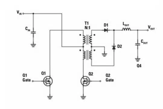
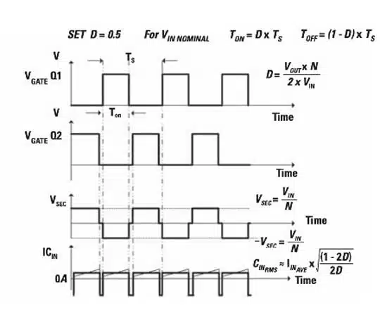
A push‑pull converter uses two switches and a transformer with a split (center‑tapped) primary; each switch alternately connects the input Vin to one half of the primary, so the transformer sees a +Vin / −Vin square waveform with dead‑time intervals.
On the secondary side, a center‑tapped rectifier converts the bipolar square wave into unidirectional pulses at twice the switching frequency, which are then smoothed by an LC output filter to generate a regulated DC output.
Because each primary leg swings against the full input, the drain‑to‑source voltage stress on each primary MOSFET is approximately 2×Vin, which directly impacts device selection, derating, and layout strategy for high‑voltage designs.
Key features and benefits
For the right power range and isolation level, push‑pull still offers several practical advantages over more complex bridge topologies:
- Simple power stage: Only two primary switches and a single transformer are required, which keeps gate‑drive circuitry straightforward and reduces BOM line items compared with a full bridge or PSFB.
- Cost‑effective controllers: Dedicated push‑pull PWM controllers are widely available and generally cheaper than PSFB controllers, which can be attractive in cost‑sensitive telecom, auxiliary or bias supplies.
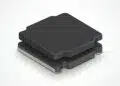
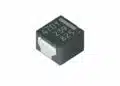
- Compact transformer: The transformer can be designed similarly to a PSFB transformer, with the main difference being the center‑tapped primary; for moderate power and good design margins this can yield compact, efficient magnetics.
- Reasonable EMI at moderate power: With fewer floating high‑dv/dt nodes than a full bridge, common‑mode EMI can be inherently lower, reducing the burden on CM chokes and Y capacitors in some applications.
However, engineers must actively manage volt‑second balance and zero‑voltage switching; these are not “self‑healing” in push‑pull and can limit the usable power and input‑voltage range if ignored.
Push‑pull vs PSFB: design trade‑offs
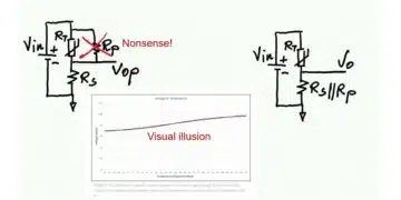
The Push-Pull converter has two switches and two primary windings in the transformer that connects Vin to each winding alternatively, generating a square +Vin and -Vin, with a zero interval waveform in the transformer.
Due to the configuration, voltage across switches is 2 x Vin. The seconday is a center tap rectifier configuration that transform the negative pulses in positives (doubling the frequency) before the L-C filter. This pulsating signal is filtered by a L-C filter generating the constant DC voltage in the output.
Transformer design and volt‑second balance
From a magnetics perspective, push‑pull and PSFB transformers look similar on paper, but their tolerance to real‑world asymmetries is very different. In both cases the designer must ensure that the average volt‑seconds per cycle on the core is zero to avoid DC flux and saturation.
In a push‑pull converter, volt‑second balance depends on the two primary intervals matching closely; any mismatch from driver delays, MOSFET parameter spread, dead‑time asymmetry or PCB layout can create a DC component in the applied flux. Over time, this can push the core toward saturation, leading to rising magnetizing current, overstress of switches, and potential catastrophic failures.
PSFB, by contrast, generates positive and negative cycles through phase‑shift modulation of the same bridge legs, so any imbalance is largely driven by layout and passive tolerances rather than inherent asymmetry in gate timing. This makes PSFB more forgiving in high‑power designs, especially when combined with digital control or well‑tuned analog controllers.
For push‑pull magnetics, practical mitigation includes:
- Generous core‑size and flux‑density margin to tolerate some DC offset without saturating.
- Tight driver matching, symmetric gate‑resistors and carefully routed gate traces to minimize timing skew.
- Careful dead‑time design so that one MOSFET fully turns off before the other turns on, without unnecessarily extending blanking time.
Zero‑voltage switching (ZVS) considerations
Modern power supplies increasingly rely on ZVS or related soft‑switching techniques to hit efficiency and thermal targets at higher frequencies. In this context, the push‑pull topology has a structural limitation: ZVS is not “built into” its commutation paths.
To achieve ZVS in any topology, two conditions are required at turn‑on:
- Sufficient inductive current at the end of the previous interval to charge and discharge node capacitances.
- A defined path during dead‑time that forces the switching node to swing and naturally commutate the MOSFET output capacitances.
In push‑pull, the transformer’s magnetizing and leakage inductance provide current, but the current is not inherently forced through the commutation path during dead‑time. As a result, any ZVS observed is accidental and strongly dependent on load, parasitics, and specific operating points; at other loads or temperatures, the same design may revert to hard‑switching with higher losses.
By comparison, PSFB intentionally routes current through the nodes that need to transition, making it possible to obtain predictable ZVS across a wider load range once the tank and timing are tuned. For teams targeting high power density or strict efficiency mandates, this is a key reason PSFB has displaced push‑pull in many mid‑ to high‑power designs.
EMI behavior
EMI performance is another recurring concern when selecting a topology and planning the input/output filter strategy. The push‑pull vs PSFB comparison in the source highlights both common‑mode (CM) and differential‑mode (DM) noise behavior.
- Push‑pull tends to generate smoother CM noise at moderate power because it has fewer floating, high‑dv/dt mid‑points; the primary is not arranged as a full bridge with a switching midpoint swinging from 0 to Vin. This can ease CM filtering, especially where tight leakage requirements to protective earth are present.
- On the other hand, the lack of natural ZVS means switching transitions are sharper, which tends to increase DM noise and may require more aggressive series inductors, RC snubbers or damping networks on the primary and secondary.
In PSFB, multiple high‑dv/dt nodes and a floating bridge midpoint make CM noise control more challenging, often requiring more sophisticated shielding, careful transformer winding structures (e.g. Faraday shields), and higher‑performance CM chokes. ZVS, however, reduces DM noise by softening transitions, which can simplify the DM section of the filter.
For EMI‑critical designs, a realistic assessment of available board area for filters, allowable leakage currents, and regulatory class (CISPR, FCC, automotive EMC, etc.) should be part of the topology decision, not an afterthought.
IC ecosystem and cost impact
The controller IC landscape has a direct impact on both engineering effort and long‑term maintainability of the design. The use of push‑pull and PSFB controllers show a clear trend:
- Push‑pull controllers are widely available, often simpler and cheaper, which is attractive when building cost‑optimized auxiliary or bias supplies, or when a design team wants a proven analog controller with minimal configuration overhead.
- PSFB controllers, while more expensive and complex, typically offer better integration for high‑power stages (advanced gate‑drive timing, configurable dead‑time, synchronous rectification support, protection features) and tend to be better supported by application notes and reference designs for demanding use cases.
One practical recommendation is to evaluate not only unit price but also the availability of solid technical support and design resources from the IC vendor; for a topology like push‑pull, where layout and timing details are critical to avoiding saturation and over‑stress, access to experienced support can be decisive.
Push-pull controller IC examples
| Vendor | IC | Notes |
|---|---|---|
| TI | UCC2808A (1,5€) | Push-pull current-mode, telecom-era |
| Analog Devices | UC1846 / UC3846 (3–5€) | Legacy |
| onsemi | NCP1568 (1,6€) | Push-pull / forward |
PSFB controller IC examples
| Vendor | IC | Notes |
|---|---|---|
| TI | UCC28950 / UCC28951 (4€) | Industry reference, adaptive dead-time |
| ADI | LT3752 / LTC3722 (5€) | High-performance bridge control |
Topology comparison for isolated DC/DC
The table below summarizes the practical implications showing contrasts of push‑pull vs phase‑shifted full bridge across several dimensions that matter to hardware teams.
| Aspect | Push‑pull | PSFB (phase‑shifted full bridge) |
|---|---|---|
| Primary switches | 2 switches, center‑tapped primary | 4 switches in full‑bridge configuration |
| Switch voltage stress | ≈ 2×Vin per MOSFET | Typically ≈ Vin per MOSFET |
| Volt‑second balance | Sensitive; relies on symmetry of two separate on‑times and hardware | More robust; positive and negative cycles set by same phase‑shift |
| ZVS behavior | Not natural; any ZVS is incidental and load‑dependent | Structural; commutation paths support ZVS over a wider load range |
| EMI tendencies | Fewer floating nodes; smoother common‑mode, more differential‑mode noise | More CM noise from floating nodes; ZVS helps DM noise |
| Controller ecosystem | Simple, low‑cost push‑pull controllers available | More complex, higher‑cost controllers, but strong support |
| Typical power window | Narrowing; small–medium power where cost dominates | Medium–high power where efficiency and thermals dominate |
| Cost and complexity | Lower switch count and simpler drivers; attractive at modest power levels | Higher part count and controller cost but better suited for high‑power, high‑efficiency designs |
For new platforms, many OEMs now reserve push‑pull for narrower ranges where its simplicity and lower controller cost still outweigh the risks around transformer saturation and non‑natural ZVS.
Typical applications
The usable range of push‑pull has narrowed over the years, but there are still application segments where it remains a competitive choice. Typical use cases include:
- Isolated auxiliary and bias supplies in larger power systems, where output power is modest and a simple, low‑cost topology is sufficient.
- Telecom or industrial control boards requiring isolated rails at tens to low hundreds of watts, especially where existing designs or magnetics platforms are already based on push‑pull.
- Legacy or derivative platforms where reuse of proven magnetics and controller circuits is more valuable than re‑architecting the power stage around PSFB or LLC.
For new clean‑sheet designs, many engineers now position push‑pull between forward/flyback (for lower power) and more advanced bridge/LLC topologies (for higher power), and only select it when cost and simplicity clearly outweigh the drawbacks around ZVS and transformer robustness.
Design‑in notes for engineers
For teams considering push‑pull in a new or updated platform, several design‑in points emerge from the analysis:
- Confirm the power and voltage window: Use push‑pull where input voltage and power level keep device voltage stress, core losses, and flux swing within comfortable margins without resorting to exotic parts.
- Over‑design the transformer for balance: Select a core size and flux density that tolerate plausible DC offsets; pay particular attention to symmetry in primary turns, winding distribution, and leakage inductance.
- Invest in symmetric gate‑drive: Use matched drivers, equal gate resistors, and mirrored routing to reduce timing skew between the two switches; this directly lowers the risk of DC flux imbalance.
- Plan for hard‑switching: Treat hard‑switching as the default mode and design snubbers, clamp networks, and thermal paths accordingly; do not rely on coincidental ZVS to meet efficiency targets.
- Prototype for EMI early: Since DM noise is likely to be significant, include placeholder footprints for RC snubbers, damping networks, and filter upgrades, and plan early bench time for conducted and radiated tests.
Where high efficiency, wide operating range, and thermal headroom are critical, PSFB or other soft‑switching topologies will usually be a better fit, but understanding the push‑pull’s behavior remains essential for maintaining and debugging existing fleets.
Conclusion
Push‑pull converters remain a valid option for isolated DC/DC stages when simplicity and low cost are more important than absolute efficiency or maximum power density, especially in auxiliary and medium‑power supplies where controller ICs and magnetics are well understood by the design team. Compared with PSFB, they demand tighter control of transformer volt‑second balance, accept hard‑switching as the default, and require more attention to differential‑mode EMI, but can reward careful design with compact, robust and cost‑effective power stages that integrate cleanly with standard passive components and EMI filters.
When choosing between push‑pull and PSFB in new platforms, engineers should weigh controller ecosystem, EMI constraints, power range and long‑term maintainability, while purchasing teams evaluate life‑cycle status and supply risk for the chosen controllers, magnetics and key passive components.
| Aspect | Push-pull | PSFB |
|---|---|---|
| Power Range | 100–500 W | 500 W–kW |
| Efficiency | Medium | High |
| ZVS Robustness | Low | Medium–High |
| Flux Balance | Sensitive | Guaranteed |
| EMI | Easier | Harder |
| Cost | Lower | Higher |
| IC Support | Limited | Strong |
FAQ: DC/DC push-pull converter vs PSFB
A DC/DC push-pull converter is an isolated power topology that uses two switches and a center-tapped transformer primary to generate a bipolar square wave, which is then rectified and filtered into a regulated DC output.
Push-pull is most attractive in low to medium power isolated supplies where simplicity, low controller cost and reuse of existing magnetics matter more than maximum efficiency or very wide operating range.
The main risks are transformer volt-second imbalance that can drive the core into saturation, higher switch voltage stress at about twice the input voltage, and the lack of natural ZVS, which leads to harder switching and higher differential-mode EMI.
Push-pull tends to have fewer floating high-dv/dt nodes, which can reduce common-mode noise, but its hard-switching transitions usually produce stronger differential-mode noise that must be handled with snubbers and well-designed input/output filters.
The transformer and its leakage and magnetizing inductance are critical, alongside well-rated MOSFETs, snubber networks, DC-link capacitors, and EMI filter components that must withstand repetitive voltage stress and switching noise.
How-to: Design-in a DC/DC push-pull converter
- Step 1: Define power and voltage requirements
Start by defining input voltage range, output power, isolation level and efficiency targets to confirm that a push-pull topology is appropriate instead of PSFB or flyback/forward alternatives.
- Step 2: Select the topology and controller IC
Choose a push-pull controller IC with suitable drive capability, protection features and supply voltage, and verify its recommended operating area and life-cycle status in the latest datasheet and distributor listings.
- Step 3: Design the transformer for volt-second balance
Design the center-tapped transformer with adequate core size and flux density margin, symmetric primary windings, and controlled leakage inductance to tolerate small DC offsets and avoid core saturation over the full operating range.
- Step 4: Dimension MOSFETs, rectifiers and passive components
Select MOSFETs rated for roughly twice the maximum input voltage plus margin, appropriately rated rectifiers, DC-link capacitors, snubbers and EMI filter components based on worst-case voltage, current and thermal conditions.
- Step 5: Optimize gate drive and PCB layout
Implement symmetric gate-drive paths with matched resistors, tight coupling to the transformer and short high-current loops, minimizing parasitic inductance and timing skew that can aggravate volt-second imbalance and switching losses.
- Step 6: Validate ZVS behavior, losses and EMI in the lab
Measure waveforms, switching losses, transformer flux behavior and conducted/radiated EMI across load, temperature and line conditions, then tune snubbers, filters and timing to ensure reliable hard-switching operation and compliance with EMC limits.
Source
This article summarizes and re‑structures the technical content of a detailed newsletter edition by Chema Molina on DC/DC push‑pull converters and their comparison to PSFB, adding context and design‑in guidance tailored for passive‑component‑focused engineers and purchasers.