Passive Components Blog
No Result
View All Result
  • Home
  • NewsFilter
    • All
    • Aerospace & Defence
    • Antenna
    • Applications
    • Automotive
    • Capacitors
    • Circuit Protection Devices
    • electro-mechanical news
    • Filters
    • Fuses
    • Inductors
    • Industrial
    • Integrated Passives
    • inter-connect news
    • Market & Supply Chain
    • Market Insights
    • Medical
    • Modelling and Simulation
    • New Materials & Supply
    • New Technologies
    • Non-linear Passives
    • Oscillators
    • Passive Sensors News
    • Resistors
    • RF & Microwave
    • Telecommunication
    • Weekly Digest

    Samsung Releases Automotive Molded 2220 1kV C0G MLCC

    How to Select Ferrite Bead for Filtering in Buck Boost Converter

    VINATech Offers Smallest 100µF Al-Hybrid Capacitor

    Vishay Unveils SMD 1200V PTC Thermistors in Compact Size

    Power Inductors Future: Minimal Losses and Compact Designs

    Bourns Unveils Automotive 3 Watt Gate Driver Transformer

    Murata Opens EMC Test Lab in Nuremberg to Enhance Automotive Support

    Percolation Phenomenon: Degradation of Molded Power Inductors in DC/DC Converters

    Molex Acquires Smiths Interconnect

    Trending Tags

    • Ripple Current
    • RF
    • Leakage Current
    • Tantalum vs Ceramic
    • Snubber
    • Low ESR
    • Feedthrough
    • Derating
    • Dielectric Constant
    • New Products
    • Market Reports
  • VideoFilter
    • All
    • Antenna videos
    • Capacitor videos
    • Circuit Protection Video
    • Filter videos
    • Fuse videos
    • Inductor videos
    • Inter-Connect Video
    • Non-linear passives videos
    • Oscillator videos
    • Passive sensors videos
    • Resistor videos

    How to Select Ferrite Bead for Filtering in Buck Boost Converter

    Power Inductors Future: Minimal Losses and Compact Designs

    Percolation Phenomenon: Degradation of Molded Power Inductors in DC/DC Converters

    Connector PCB Design Challenges

    Efficient Power Converters: Duty Cycle vs Conduction Losses

    Ripple Steering in Coupled Inductors: SEPIC Case

    SEPIC Converter with Coupled and Uncoupled Inductors

    Coupled Inductors in SEPIC versus Flyback Converters

    Non-Linear MLCC Class II Capacitor Measurements Challenges

    Trending Tags

    • Capacitors explained
    • Inductors explained
    • Resistors explained
    • Filters explained
    • Application Video Guidelines
    • EMC
    • New Products
    • Ripple Current
    • Simulation
    • Tantalum vs Ceramic
  • Knowledge Blog
  • Suppliers
    • Who is Who
  • PCNS
    • PCNS 2025
    • PCNS 2023
    • PCNS 2021
    • PCNS 2019
    • PCNS 2017
  • Events
No Result
View All Result
Passive Components Blog
No Result
View All Result

KYOCERA to Build New Plant in Kagoshima, Japan, for Ceramic Microelectronic Packages

3.5.2018
Reading Time: 2 mins read
A A

Source: Kyocera news

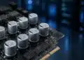
New facility will produce ceramic packages for electronic and semiconductor components, including SMD and CMOS devices, to support IoT growth.
March 29, 2018
Kyocera Corporation (President: Hideo Tanimoto) announced today that it will construct a new manufacturing plant on the premises of its Kagoshima Sendai manufacturing complex to increase production of ceramic microelectronic packages. The company entered into a site location agreement with local governments, and a signing ceremony was held March 16 at the Satsumasendai municipal office in the presence of the governor of Kagoshima Prefecture and mayor of Satsumasendai. Construction is scheduled to begin in April 2018 for the new plant, which will be the 22nd facility at Kyocera’s Kagoshima Sendai manufacturing complex.

RelatedPosts

Samsung Releases Automotive Molded 2220 1kV C0G MLCC

How to Select Ferrite Bead for Filtering in Buck Boost Converter

VINATech Offers Smallest 100µF Al-Hybrid Capacitor

The new facility, which Kyocera plans to open in August 2019, will bring a 25 percent increase in the company’s total production capacity for ceramic packages used to house SMD*1 electronic devices and CMOS*2 image sensors.

Kyocera’s heritage is rooted in ceramics – the company’s name is derived from Kyoto and ceramic. In 1959, Kyocera began manufacturing ceramic insulators for TV picture tubes and later became the world leader in fine (advanced) ceramics, producing electronic components, semiconductor process components, and parts for LCDs and LEDs, among other applications. The company’s original Kagoshima Sendai Plant opened in 1969 to produce multilayer ceramic packages for ICs used in desktop calculators.

The electronics industry is now experiencing new growth fueled by big data, artificial intelligence, and the Internet of Things (IoT). The development of advanced driver-assist systems (ADAS) and technology that supports minimally invasive medical treatments will drive future growth as well. The new Sendai facility will significantly increase Kyocera’s production capacity for two key enablers of these applications — SMD ceramic packages and packages to house CMOS image sensors — as well as ceramic packages for automotive and medical devices.

Kyocera’s investment will contribute to Kagoshima’s local economy, strengthening the supply chain for semiconductor components and creating job opportunities in the area.

Details of the New Plant

Name Kyocera Corporation Kagoshima Sendai Plant (the 22nd facility on the premises)
Location On the premises of Kyocera’s existing Kagoshima Sendai Plant,
1810 Taki-cho Satsumasendai, Kagoshima 895-0292 Japan
Total investment Approximately 5.5 billion yen (approx. USD 52.4 million)
Building area 8,235m2 steel construction with 6 stories
Total floor space 42,283m2
Construction plan Begin construction: April 2018; start manufacturing: August 2019
Main products SMD ceramic packages, ceramic packages for CMOS image sensors
First-year production plan Approximately 3.8 billion yen (from August 2019 through March 2020)

*1 SMD: Surface-mount device
*2 CMOS: Complementary metal oxide semiconductor

featured image credit: Kyocera, architect rending picture

Related

Recent Posts

Murata Opens EMC Test Lab in Nuremberg to Enhance Automotive Support

22.10.2025
10

Molex Acquires Smiths Interconnect

21.10.2025
9

September 2025 ECIA US Components Sales Sentiment Continues in Optimism

20.10.2025
19

Vishay Expanded Inductor Portfolio With More Than 2000 Stock Items 

8.10.2025
24

Paumanok Releases Capacitor Foils Market Report 2025-2030

7.10.2025
30

Advancements in Flexible End Terminations for Robust MLCCs in EV

26.9.2025
49

Passive Components J-STD-075 Process Sensitivity Level Classification And Labeling

25.9.2025
73

AI Hardware Development and Its Consequences for Passive Electronic Components

23.10.2025
126

Samtec Agreed with Molex Second-Source License on High-Speed Interconnects for Data Centers

18.9.2025
24

August 2025 ECIA US Components Sales Sentiment Remains Strong

18.9.2025
46

Upcoming Events

Oct 28
8:00 - 15:00 CET

Power Up Your Design: SN6507 and the Ready-to-Use Development Kit

Oct 30
11:00 - 12:00 CET

Space Ceramic Capacitors with Flexible Testing

Nov 4
10:00 - 11:00 PST

Design and Stability Analysis of GaN Power Amplifiers using Advanced Simulation Tools

View Calendar

Popular Posts

  • Buck Converter Design and Calculation

    0 shares
    Share 0 Tweet 0
  • Boost Converter Design and Calculation

    0 shares
    Share 0 Tweet 0
  • LLC Resonant Converter Design and Calculation

    0 shares
    Share 0 Tweet 0
  • Flyback Converter Design and Calculation

    0 shares
    Share 0 Tweet 0
  • Ripple Current and its Effects on the Performance of Capacitors

    3 shares
    Share 3 Tweet 0
  • What is a Dielectric Constant and DF of Plastic Materials?

    4 shares
    Share 4 Tweet 0
  • SEPIC Converter Design and Calculation

    0 shares
    Share 0 Tweet 0
  • MLCC and Ceramic Capacitors

    0 shares
    Share 0 Tweet 0
  • Dual Active Bridge (DAB) Topology

    0 shares
    Share 0 Tweet 0
  • Flying Capacitors

    0 shares
    Share 0 Tweet 0

Newsletter Subscription


Passive Components Blog

© EPCI - Leading Passive Components Educational and Information Site

  • Home
  • Privacy Policy
  • EPCI Membership & Advertisement
  • About

No Result
View All Result
  • Home
  • Knowledge Blog
  • PCNS

© EPCI - Leading Passive Components Educational and Information Site

This website uses cookies. By continuing to use this website you are giving consent to cookies being used. Visit our Privacy and Cookie Policy.
Go to mobile version