


This paper explains layer-by-layer fabrication method, where nanocomposite dielectrics are printed by successive depositions of ultra-thin layers of a room-temperature-stable polymer ink. The work explores two polypropylene-based inks in industry-friendly solvents that are then used to fabricate capacitor devices.
The paper was presented by William Greenbank, Centre for Industrial Electronics, SDU University of Southern Denmark, Denmark at the 4th PCNS 10-14th September 2023, Sønderborg, Denmark as paper No. 4.3. and selected by TPC Technical Program Committee as:
OUTSTANDING PAPER AWARD
Introduction
Electricity generation accounts for 47% of all new carbon emissions because electricity production is expected to increase by 80% by 2040 – a significant portion from fossil fuel sources. It is therefore necessary to both kerb rising demand for energy and increase renewable energy’s share of electricity generation to have any realistic hope of reducing emissions long-term. More efficient power electronics can have an enormous impact on energy wastage. Capacitors are critical to the operation of power electronics, but often the weak link when it comes to efficiency improvements. This is particularly true for electric motors, which account for 40% of all global electricity consumption and this will only increase as electric vehicles become more prevalent. Reducing energy waste in motors requires that their drives are smaller and can tolerate higher temperatures while remaining highly reliable and stable at high voltages. However, existing dielectric materials cannot deliver a capacitor that meets all of these requirements. See Figure.1. in an example of DC-link power capacitor considerations.

Nanocomposite dielectrics are an increasingly important area of innovation in capacitor research as an avenue to improve capacitive energy density, electrical breakdown strength, and temperature stability of devices. In such devices, morphology control is critical in order to optimise electrical field distribution in the device and to prevent the clustering of nanoparticles lowering breakdown voltages. However, this is difficult to achieve with large-scale fabrication techniques, such as melt extrusion and stretching, as melt processing can induce clustering and offers few possibilities for fine structure control of length scales below 1 µm.
Layer-by-layer fabrication offers a potential bottom-up alternative whereby dielectrics are printed by successive depositions of ultra-thin layers of a room-temperature-stable polymer ink. This would allow fine thickness and morphology control and could easily be adapted to industrial-scale printing techniques, like roll-to-roll slot-die coating. Our work explores the potential of this technique by developing two polypropylene-based inks in industry-friendly solvents that are then used to fabricate capacitor devices. A gel ink was able to be used to deposit ultrathin (sub-200 nm) layers of mostly amorphous polypropylene with high reproducibility. Capacitors based on these polypropylene layers perform commensurate with commercial devices, exhibiting excellent self-clearing and breakdown performance. Successive depositions of the ink were also demonstrated, allowing the fabrication of devices with finely tuned thicknesses and capacitances, as well as nanocomposite capacitors. This demonstrates the viability of layer-by-layer dielectric printing and paves the way for commercial ultra-thin conformable polypropylene capacitors, multi-component sandwich nanocomposite capacitors, and multilayer polypropylene film capacitors, as well as brand new possibilities in dielectrics research.
Overview of Nanocomposite Capacitors
In the context of power capacitors, nanocomposite dielectrics are typically envisaged as a polymer matrix/continuous phase containing one or more ceramic nanomaterials (materials with at least 1 dimension in the 1 – 100 nm length scale).[7] A representation of this and some of the different material possibilities are shown in Figure 2.
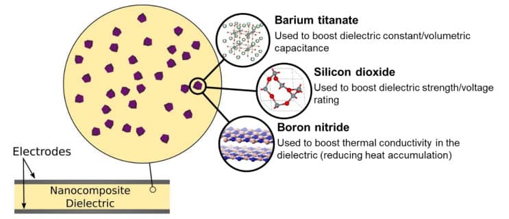
Different nanomaterials may be used to enhance different dielectric properties, such as high-εr materials to boost the volumetric/specific capacitance of the device,[8] high dielectric strength materials to boost breakdown voltage,[9] thermally conductive materials to remove heat from the device,[10] and conductive materials to reduce dissipation factor.[11] While individually effective, these nano-dopants are most effective when used together in multi-material systems, such as sandwich dielectrics[12]–[14] which include alternating layers doped with either high-εr nanoparticles or high-dielectric strength nanoparticles, in order that the best combination of dielectric properties can be achieved.
Challenges in Nanocomposite Capacitor Fabrication
Such a seemingly simple solution to dielectric material engineering should already be well established in the capacitor market, however commercial nanocomposite capacitors are practically non-existent. This is because numerous challenges exist in their fabrication. When placed in a polymer matrix, ceramic nanoparticles have a tendency to cluster, driven by a high interfacial energy between the particle and the polymer and therefore a thermodynamic driving force towards reducing the area of the interface by clustering.[15]
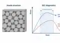
The formation of nanoparticle clusters in a nanocomposite dielectric has several important consequences. First is that the dielectric properties of the particles do not transfer well to the nanocomposite,[8] but perhaps more important is that such clusters can act as defect sites for dielectric breakdown.[16], [17] The maximum energy density of a parallel-plate capacitor is given in equation (1):
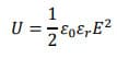
In which U is the maximum energy density (per unit volume) and E is the breakdown field strength (voltage/unit thickness). Therefore, any potential gain in energy density is completely undone if clustering causes even a slight decline in breakdown voltage.
Furthermore, nanomaterials pose significant challenges for device fabrication. The vast majority of metallised film capacitors are fabricated by extruding and stretching the dielectric polymer from a melt (e.g., biaxially oriented polypropylene – BOPP).[18], [19] Nanoparticles added to a hot polymer melt have decreased kinetic stabilisation owing to the heat of the melt, increasing the likelihood of clustering, which can decrease the quality of the extruded film.[20] Such clusters also act as fracture initiation sites during stretching, limiting the extent to which stretching can be used to decrease film thickness and orient the polymer.[21]
Layer-by-Layer Nanocomposite Dielectric Fabrication
At the University of Southern Denmark Centre for Industrial Electronics we have developed a layer-by-layer printing method for fabricating nanocomposite dielectrics for capacitors (Figure 3(1-4)).[22] This technique will utilise standard industrial-scale printing methods, such as roll-to-roll slot die coating, to deposit layers of polymer or polymer/nanocomposite dielectrics utilising novel polymer gel inks based on industry-friendly solvents.[22] In addition to offering unparalleled thickness and morphology control, this technique permits the commercial scale production of numerous different device architectures which would be impractical or impossible using extrusion-based fabrication (Figure 3(5-7)).[22] This includes the “sandwich dielectric” which is favoured by researchers for the implementation of nanocomposite dielectrics.[12]–[14]
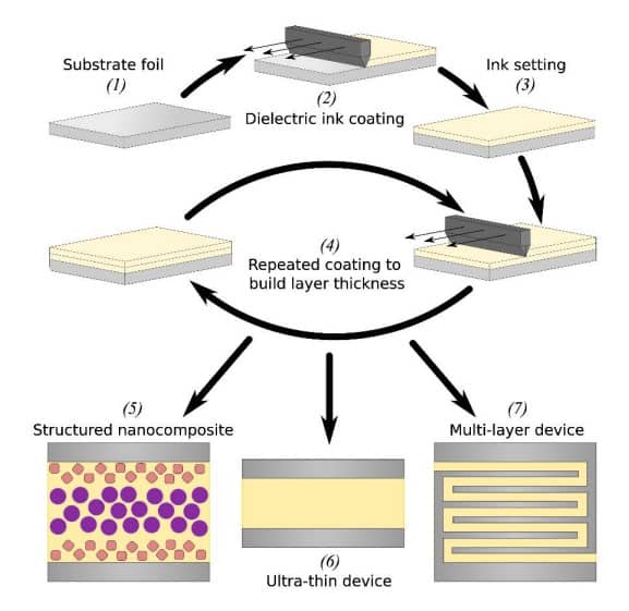
A series of prototype devices were printed with this technique based on polypropylene. The devices printed without the inclusion of nanoparticles exhibited predictable and reproducible capacitances and thicknesses, with dielectric properties comparable with commercial polypropylene.[22] Sandwich-like devices were also fabricated with alternating layers of pure polypropylene and polypropylene doped with barium titanate nanoparticles (Note: barium titanate is basic dielectric of class II. ceramic capacitors). These devices exhibited a 20% improvement in dielectric constant with no significant decline in breakdown voltage with the addition of only 0.77% (v/v) BaTiO3 nanoparticles.[22] This is in good agreement with recent theoretical findings, which indicate that even greater improvements in dielectric constant are attainable without sacrificing breakdown performance.[23]–[25]
Future Perspectives
Layer-by-layer dielectric printing is an enabling technique that opens the door to a range of new research pathways and commercial capacitor design possibilities. With this technology, manufacturers will have the ability to design nanocomposite dielectric morphologies for specific applications. Moreover, the controlled fabrication of reliable nanocomposite capacitors will allow the promises of more compact, high temperature stable capacitors to be realised, decreasing the size of motor drives and facilitating the transition to high-efficiency wide band-gap semiconductor-based power electronics in e-mobility applications.
One thing that has been emphasised in this work and others is the importance of nanoparticle surface engineering, both from the perspective of preventing nanoparticle clustering and in promoting good transfer of dielectric properties from the dopant ceramic to the nanocomposite.[8], [26] This is an area of ongoing research that is expected to bear fruit in the near future. In addition to nanoparticles, the possibility of using other additives, such as cross-linking agents to improve the thermal resiliency of the layer is made possible with this technique, as well as the systematic study of the effects of different nano-dopants in a controlled/systematic fashion in an industry-relevant setting. Finally, the scalability of this technique will be explored, with the first trials of commercial-scale printing anticipated in 2024.
Read the Full Paper
For details on the layer-by-layer nanocomposite printing technique outlined in this summary, the reader is referred to:
Greenbank, W., & Ebel, T. (2023). Layer-by-layer printable nano-scale polypropylene for precise control of nanocomposite capacitor dielectric morphologies in metallised film capacitors. Power Electronic Devices and Components, 4, 100025.