


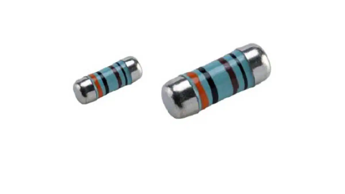
MELF stands for Metal Electrode Leadless Face, a type of surface mount device (SMD) that features a distinctive cylindrical shape. Unlike traditional rectangular chip resistors, MELF resistors have a leadless, barrel-shaped design with metal end caps that serve as the electrical termination points.
Key Takeaways
- MELF resistors feature a cylindrical leadless design, offering improved stability and reliability over traditional chip resistors.
- They provide a wide resistance range, low noise characteristics, and excellent thermal and electrical properties for diverse applications.
- MELF resistors excel in demanding environments, such as automotive, medical, and industrial applications due to their high reliability and low failure rates.
- The manufacturing process involves precise film deposition and laser trimming for tight tolerances and minimal inductance.
- MELF resistors outperform chip resistors in accuracy, heat dissipation, and high-frequency performance, justifying their higher cost.
What is a MELF Resistor?
The MELF resistor consists of a high-grade ceramic body onto which a resistive film is deposited. This film can be metal film, carbon film, or metal glaze, depending on the application requirements. The ceramic core is then fitted with nickel-plated steel termination caps, which are pressed onto the metallized ends of the resistive element. A protective coating covers the entire assembly, providing electrical, mechanical, and climatic protection.
The cylindrical construction of MELF resistors offers several key advantages over flat chip resistors, particularly in terms of stability, reliability, and power handling capabilities.
Solderability is vital for a successful result. The user should use a wetting balance and international standard requirements at inspection. The end caps of MELFs sometimes have been difficult to solder. Metal glaze MELFs with metallized terminations generally have a better solderability.
Because the MELF design is a modified version of well-tried, well-established hole mount types, it in this SMD component assimilates all the good characteristics that characterize the respective basic hole mount type.
For metal film MELF this means among other things
- a wide resistance range
- low noise characteristics
- fine tolerances
- low TCR values
- good stability
With an extra thick metal film one has in some cases improved heat dissipation and also pulse capability. High frequency capability is achieved by a so called pulsed trim cut where the spiraled conductive pattern is broken in parts, thus reducing the inductive action from the helical trim cut and thus increasing the frequency range to several GHz.
MELF components are made in metal film, carbon film and metal glaze types. Usually they are supplied with end caps of conventional components but some manufacturers use metallized terminations.
Sizes
The MELF components were introduced as leadless metal film resistors in the DIN size 0207. Today 0204 (1.5 x 3.6 mm) is the most common, not least because of its smaller risk of open mode failure in the solder joints after frequent temperature changes. However, the size 0102 (1.1 x 2.2 mm) is already well established in the consumer market.
MELF resistors are available in various sizes and specifications to meet different application requirements.
0102 (Mini-MELF): 1.1 x 2.2 mm – The smallest MELF size, well-established in consumer markets. Offers reduced risk of open-mode failure in solder joints.
0204 (Mini-MELF): 1.5 x 3.6 mm – The most common size today, providing an excellent balance between size and reliability. Features lower risk of solder joint failures after temperature cycling.
0207 (MELF): 2.2 x 5.8 mm – The original MELF size introduced with DIN standards, offering higher power ratings and better heat dissipation.
MELF Size Comparison Table
| Size Designation | Dimensions (mm) | DIN Size | Metric Code | Typical Power | Key Features |
|---|---|---|---|---|---|
| 0102 (Mini-MELF) | 1.1 x 2.2 | – | RC2211M | 0.2-0.3W | Smallest size, excellent for high-density PCBs |
| 0204 (Mini-MELF) | 1.5 x 3.6 | 0204 | RC3715M | 0.25-0.4W | Most common, best balance of size and reliability |
| 0207 (MELF) | 2.2 x 5.8 | 0207 | RC6123M | 0.4-1.0W | Original size, highest power ratingDisadvantages of MELF Comparative Analysis |
MELF Resistor Construction and Manufacturing
The manufacturing process of MELF resistors is precise and highly controlled, which directly contributes to their superior performance characteristics.
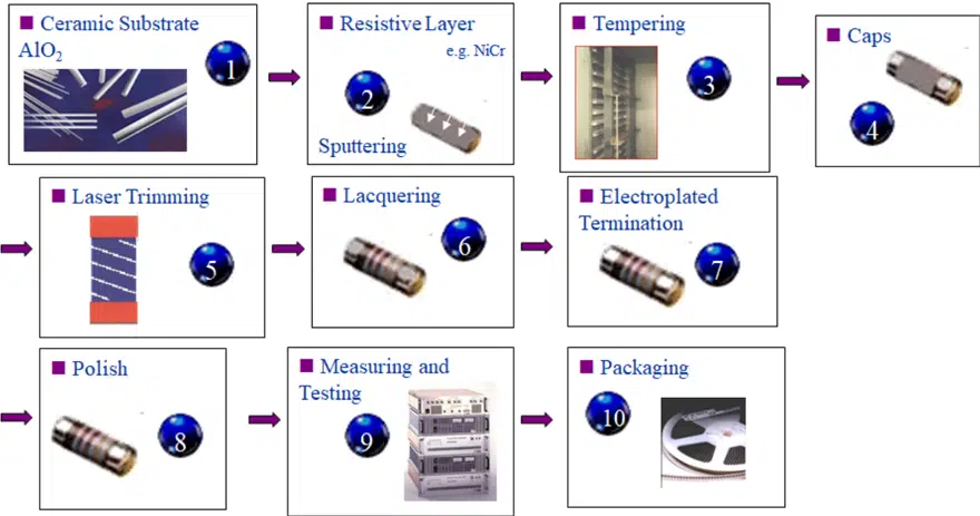
Core Construction
The foundation of a MELF resistor is a high-grade ceramic rod that provides excellent thermal and electrical properties. The ceramic material offers dimensional stability across a wide temperature range and serves as an ideal substrate for the resistive element.
Film Deposition
Depending on the type of MELF resistor, different film deposition techniques are used:
Metal Film MELFs: A thin layer of metal alloy is deposited onto the ceramic body through sputtering in a tightly controlled vacuum chamber. The metal targets contain precisely controlled ratios of metallic elements to produce the desired resistance characteristics. This sputtering process creates a very dense and uniform resistive film that is approximately 1000 times thinner than thick film elements.
Carbon Film MELFs: A carbon-based resistive material is deposited onto the ceramic substrate, offering good performance for general applications at a lower cost than metal film versions.
Metal Glaze MELFs: A metal glaze mixture is applied to the ceramic body and then fired at high temperatures to form the resistive element.
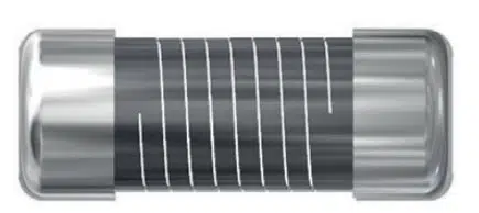
Laser Trimming
After the resistive film is deposited, a special laser cuts a helical groove into the resistive layer. This precision trimming process adjusts the resistance to the exact target value with very tight tolerances (down to ±0.1% or better). The helical pattern also helps minimize inductance, making MELF resistors suitable for high-frequency applications.
Termination and Protection
Nickel-plated steel termination caps are pressed onto the metallized ends of the resistive element. These end caps are then coated with pure tin plating to ensure excellent solderability in both lead-free and lead-containing assembly processes. Finally, a protective coating is applied over the entire resistor body to provide protection against environmental factors, moisture, and mechanical stress
Resistance Range
MELF resistors offer extremely wide resistance ranges depending on the film type and size:
- Metal Film: Typically 0.16 Ω to 10 MΩ
- Carbon Film: 8.2 Ω to 1 MΩ
- Metal Glaze: 10 Ω to 100 kΩ
- Zero Ohm Jumpers: Also available as cross-over/jumper resistors with ≤10 mΩ resistance
Tolerance
MELF resistors are available with extremely tight tolerances:
- ±5% (standard)
- ±1% (precision)
- ±0.5% (high precision)
- ±0.25% (very high precision)
- ±0.1% (ultra-high precision)
Temperature Coefficient (TCR)
Metal film MELFs offer excellent TCR values:
- ±50 ppm/°C (standard)
- ±25 ppm/°C (precision)
- ±15 ppm/°C (high precision)
- ±10 ppm/°C (ultra-high precision)
Power Ratings
Power ratings vary by size and design:
- 0102: 0.2W to 0.3W
- 0204: 0.25W to 0.4W
- 0207: 0.4W to 1.0W
Operating Temperature Range
MELF resistors typically operate across -55°C to +155°C, making them suitable for harsh automotive and industrial environments.
Maximum Operating Voltage
Voltage ratings range from 150V to 500V depending on size and resistance value..
Key Advantages of MELF Resistors
MELF resistors offer several significant advantages over traditional chip resistors, making them the preferred choice for demanding applications.
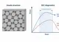
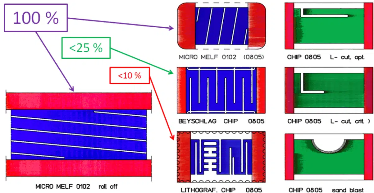
MELF capacitors that are also available in (micro)-chip case sizes have its advantage with possible path around the whole chip that makes it more efficient compare to Thick/Thin film SMDs. See the current path example on 0805 chip equivalent in Figure 3. below and pulse load capability comparison in Figure 4.:
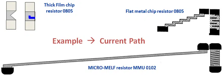
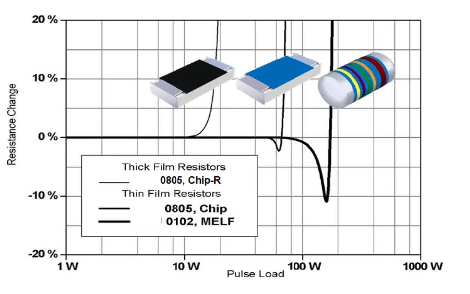
The differences in effective current length path are also reflected in the possible surface loads [W/mm2]. See the Figure 5. below.
Superior Accuracy and Stability
The cylindrical construction and metal film technology enable:
- Tighter manufacturing tolerances down to ±0.1%
- More uniform resistive film deposition
- Exceptional long-term stability with minimal resistance drift
- Less variation across production batches
Enhanced Reliability
MELF resistors demonstrate superior reliability characteristics:
- Thermal Shock Resistance: The cylindrical shape reduces stress concentrations during thermal cycling
- Vibration Resistance: Robust mechanical construction withstands harsh environments
- Moisture Resistance: Excellent protection against humidity and environmental factors
- Low Failure Rate: Observed failure rate of FIT ≤ 0.1 × 10⁻⁹/h
Excellent Pulse Load Capability
MELF resistors can handle significantly higher pulse loads than chip resistors:
- Standard versions: 2.5× power rating for 5 seconds
- Special high-pulse versions: Up to 70W continuous pulse capability
- Superior energy absorption in surge protection applications
Superior Heat Dissipation
The cylindrical geometry provides:
- Larger effective surface area for heat dissipation
- More efficient thermal transfer to the PCB
- Better power handling for given footprint
- Reduced thermal stress on the component
High-Frequency Performance
Helical laser trimming pattern minimizes parasitic inductance, enabling:
- Operation at frequencies up to several GHz
- Low noise characteristics
- Minimal signal distortion
- Excellent high-frequency stability
Low Noise Characteristics
Metal film MELFs exhibit extremely low current noise, making them ideal for precision measurement and audio applications.
Applications of MELF Resistors
MELF resistors are widely used in applications where reliability, precision, and performance are critical.
Automotive Electronics
- Engine control units (ECU)
- Anti-lock braking systems (ABS)
- Airbag systems
- Battery management systems
- Sensor circuits
- Power steering controllers
Automotive applications benefit from MELF resistors’ ability to withstand thermal cycling, vibration, and harsh environmental conditions. AEC-Q200 qualified MELF resistors meet stringent automotive quality standards.
Telecommunications
- Base station equipment
- Network infrastructure
- RF and microwave circuits
- Signal processing equipment
- Impedance matching networks
The low inductance and high-frequency capabilities make MELF resistors ideal for telecommunications applications.
Medical Equipment
- Patient monitoring systems
- Diagnostic equipment
- Imaging systems
- Precision measurement instruments
- Life-support equipment
Medical applications require the exceptional reliability and long-term stability that MELF resistors provide.
Industrial Control Systems
- Process control instrumentation
- Power supply circuits
- Motor controllers
- Automation equipment
- Measurement and testing systems
Aerospace and Defense
- Avionics systems
- Navigation equipment
- Radar systems
- Satellite communications
- Military electronics
These demanding applications benefit from MELF resistors’ proven reliability and performance under extreme conditions.
Consumer Electronics (Premium Applications)
- High-end audio equipment
- Professional video equipment
- Gaming systems
- Precision timing circuits
MELF vs. Chip Resistors: Comparative Analysis
Understanding the differences between MELF and standard chip resistors helps in selecting the right component for your application.
Advantages of MELF Resistors
Performance:
- Superior long-term stability and accuracy
- Better temperature coefficient (TCR)
- Lower noise characteristics
- Higher pulse load capability
- Better high-frequency performance
- More efficient heat dissipation
Reliability:
- Enhanced resistance to thermal shock
- Better vibration and mechanical stress resistance
- Lower failure rates in harsh environments
- Superior moisture resistance
- More predictable failure modes
Disadvantages of MELF Resistors
Manufacturing Challenges:
- Cylindrical shape can roll during pick-and-place operations
- Requires special nozzles and handling equipment
- More complex assembly process
- Higher risk of component movement before reflow
Cost Considerations:
- Generally 30-50% more expensive than chip resistors (approximately 2:3 ratio for hole-mount to MELF)
- Higher assembly costs due to specialized handling
- May require additional fixturing or glue dots
Size:
- Slightly larger footprint for equivalent power rating
- Height profile may be higher than ultra-thin chip resistors
When to Choose MELF Resistors
MELF resistors are the preferred choice when:
- High reliability is critical (automotive, medical, aerospace)
- Tight tolerances are required (≤±0.5%)
- Low TCR is essential (≤±25 ppm/°C)
- High pulse loads must be handled
- Long-term stability is paramount
- Operating in harsh environmental conditions
- High-frequency performance is needed
- Low noise is critical
When Chip Resistors May Be Sufficient
- Cost-sensitive consumer applications
- Standard tolerance requirements (≥5%)
- General-purpose circuits
- Low-power applications
- When automated assembly simplicity is prioritized
Assembly and Soldering Considerations
Proper assembly techniques are essential for successful MELF resistor implementation.
PCB Land Pattern Design
- Symmetric pad design helps prevent component rolling
- Recommended pad extension: 0.1-0.2mm beyond component end
- Avoid excessive solder paste that can cause swimming
- Use solder mask dams between closely spaced components
Pick-and-Place Handling
Equipment Requirements:
- Use cylindrical or V-groove nozzles specifically designed for MELF components
- Ensure proper vacuum pressure settings
- Implement vision alignment systems for accurate placement
- Consider using adhesive dots for components on wave-soldering side
Best Practices:
- Position components with sufficient spacing to prevent rolling contact
- Apply slight pressure during placement to embed in solder paste
- Consider component orientation relative to reflow direction
- Use fixtures or rails on PCB edges if necessary
Soldering Methods
Reflow Soldering:
- MELF resistors are fully compatible with standard SMT reflow profiles
- Both lead-free and lead-containing processes supported
- Recommended peak temperature: 245-260°C for lead-free
- Preheat rate: 1-3°C/second
Wave Soldering:
- Requires adhesive (epoxy) to secure component to board
- Position adhesive dot at component center
- Ensure component body is positioned with glue lump to substrate
- Monitor adhesive cure before wave soldering
Solderability
MELF resistors with metallized terminations generally offer better solderability than metal glaze end caps. The pure tin plating on nickel-plated steel caps provides excellent wetting. Users should:
- Use wetting balance testing per international standards
- Inspect end caps for proper solder coverage
- Follow IPC standards for solder joint quality
- Consider nitrogen atmosphere for improved results
Quality Standards and Certifications
MELF resistors from major manufacturers meet stringent international quality standards.
Automotive Standards
AEC-Q200: Automotive Electronics Council qualification for passive components
- Stress test qualification for automotive applications
- Temperature cycling requirements
- Moisture resistance testing
- Mechanical shock and vibration testing
- Essential for automotive-grade components
International Standards
EN 60115-1: Generic specification for fixed resistors
- Defines test methods and requirements
- Pulse load rating specifications
- Environmental testing protocols
EN 140401-803: Sectional specification for surface mount fixed resistors
- Quality assessment procedures
- Detailed performance requirements
IPC Standards:
- IPC-A-610: Acceptability of Electronic Assemblies
- IPC-7351: Generic Requirements for Surface Mount Design and Land Pattern Standard
Reliability Metrics
Failure Rate (FIT):
- High-quality MELF resistors: FIT ≤ 0.1 × 10⁻⁹/h
- Demonstrated through extensive life testing
- Well-defined failure modes for predictable behavior
Environmental Testing:
- Temperature cycling: -55°C to +155°C
- Humidity resistance: 85°C/85% RH
- Salt spray testing for corrosion resistance
- Vibration and mechanical shock testing
Conclusion
MELF resistors represent a mature and proven technology that continues to be the preferred choice for high-reliability applications. While they present some assembly challenges compared to standard chip resistors, their superior performance characteristics make them indispensable in demanding environments.
The key takeaways for MELF resistors include:
- Superior Performance: Exceptional accuracy, stability, and low noise make them ideal for precision applications
- High Reliability: Proven track record in automotive, medical, aerospace, and industrial applications with extremely low failure rates
- Excellent Specifications: Wide resistance ranges, tight tolerances down to ±0.1%, and low TCR values to ±10 ppm/°C
- Robust Construction: Cylindrical design provides superior resistance to thermal shock, vibration, and environmental stress
- Versatile Applications: From high-frequency RF circuits to precision measurement instruments, MELF resistors excel across diverse applications
When designing circuits for demanding applications where reliability, precision, and long-term stability are paramount, MELF resistors offer proven performance that justifies their higher cost. The investment in MELF technology pays dividends through reduced field failures, extended product lifetime, and consistent performance under harsh operating conditions.
As electronics continue to push into more challenging environments and applications require ever-greater reliability, MELF resistors remain an essential component in the engineer’s toolkit, combining the best characteristics of through-hole resistors with the space efficiency of surface-mount technology.

FAQ: MELF Resistor
MELF stands for Metal Electrode Leadless Face. It’s a surface mount device (SMD) with a distinctive cylindrical shape. Unlike traditional rectangular chip resistors, MELF resistors have a leadless, barrel-shaped design with metal end caps serving as electrical termination points. The ceramic body features a deposited resistive film (metal, carbon, or metal glaze) and offers superior stability and reliability.
MELF resistors offer exceptional long-term stability with tolerances down to ±0.1%, superior temperature coefficients (±10 ppm/°C), excellent pulse load capability up to 70W, better heat dissipation due to cylindrical geometry, high-frequency performance up to several GHz, enhanced thermal shock resistance, and extremely low failure rates (FIT ≤ 0.1 × 10⁻⁹/h).
The three standard sizes are: 0102 (Mini-MELF) at 1.1×2.2mm with 0.2-0.3W power rating, 0204 (Mini-MELF) at 1.5×3.6mm with 0.25-0.4W (most common size), and 0207 (MELF) at 2.2×5.8mm with 0.4-1.0W (original size with highest power rating).
Metal film MELF resistors typically range from 0.16Ω to 10MΩ, carbon film types from 8.2Ω to 1MΩ, and metal glaze versions from 10Ω to 100kΩ. Zero-ohm jumper versions are also available with resistance ≤10mΩ.
The main disadvantages include: cylindrical shape can roll during pick-and-place operations requiring special nozzles and handling equipment, generally 30-50% more expensive than chip resistors, higher assembly costs, more complex assembly process, and slightly larger footprint for equivalent power rating.
Choose MELF resistors when you need high reliability (automotive, medical, aerospace applications), tight tolerances (≤±0.5%), low TCR (≤±25 ppm/°C), high pulse load handling, long-term stability, operation in harsh environmental conditions, high-frequency performance, or low noise characteristics.
MELF resistors typically operate across -55°C to +155°C, making them suitable for harsh automotive and industrial environments with excellent thermal cycling resistance.
Yes, MELF resistors are ideal for automotive applications. They meet AEC-Q200 qualification standards and are used extensively in engine control units (ECU), anti-lock braking systems (ABS), airbag systems, battery management systems, and sensor circuits due to their ability to withstand thermal cycling, vibration, and harsh environmental conditions.
How to Select and Implement MELF Resistors
- Determine Your Application Requirements
Identify the critical specifications for your application including required resistance value, tolerance, temperature coefficient (TCR), power rating, operating temperature range, and environmental conditions. Consider whether your application demands high reliability (automotive, medical, aerospace), tight tolerances, or high pulse load capability.
- Select the Appropriate MELF Size
Choose from standard sizes: 0102 (1.1×2.2mm, 0.2-0.3W) for high-density applications, 0204 (1.5×3.6mm, 0.25-0.4W) for the best balance of size and reliability, or 0207 (2.2×5.8mm, 0.4-1.0W) for higher power requirements. The 0204 size is most common and offers lower risk of solder joint failures.
- Choose the Film Type
Select metal film for wide resistance ranges (0.16Ω-10MΩ), precision applications, and low noise; carbon film for general applications (8.2Ω-1MΩ) at lower cost; or metal glaze (10Ω-100kΩ) for specific requirements. Metal film offers the best overall performance characteristics.
- Design PCB Land Patterns
Create symmetric pad designs with 0.1-0.2mm extension beyond component ends. Use solder mask dams between closely spaced components. Avoid excessive solder paste that can cause component swimming during reflow. Proper land pattern design prevents rolling issues.
- Prepare Pick-and-Place Equipment
Use cylindrical or V-groove nozzles specifically designed for MELF components. Ensure proper vacuum pressure settings and implement vision alignment systems for accurate placement. Consider using adhesive dots for components on wave-soldering side. Position components with sufficient spacing to prevent rolling contact.
- Apply Soldering Process
Use standard SMT reflow profiles with peak temperature of 245-260°C for lead-free solder. Maintain preheat rate of 1-3°C/second. For wave soldering, secure components with adhesive (epoxy) at component center before processing. MELF resistors with metallized terminations offer excellent solderability.
- Inspect and Verify
Use wetting balance testing per IPC standards to verify solder joint quality. Inspect end caps for proper solder coverage. Check for proper component orientation and absence of rolling. Verify electrical resistance values are within specification after assembly.