





This guide summarizes design‑relevant aspects of thin film, metal film and metal foil resistors, with emphasis on selection, derating and PCB implementation.
Key Takeaways
- Thin Film Resistor offers precision and stability, making them ideal for applications requiring low noise and long-term reliability.
- These resistors are typically made from a homogeneous metallic alloy and are used in circuits like precision amplifiers and RC networks.
- Metal foil resistors provide the highest precision, while standard metal film covers mainstream needs, and thick film is the low-cost option.
- Careful PCB layout and derating are crucial to optimize performance and stability in demanding applications.
- Selecting between thin and thick film resistors involves balancing cost, tolerance, and application requirements.
Resistor Technology Landscape
Film resistors belong to a broader landscape of resistor technologies, each serving different roles in circuits.
- Thin and metal film resistors sit in the precision tier, combining tight tolerance, low TCR and low noise for analog and measurement designs.
- Bulk metal foil resistors occupy the ultra‑precision niche, where sub‑ppm TCR and minimal drift are critical (metrology, reference modules).
- Thick film and carbon technologies are general‑purpose workhorses, optimized for cost and very wide resistance range rather than ultimate precision.
- Wirewound and metal oxide film resistors serve high‑power and high‑temperature applications where hotspot temperatures well above 155 °C are acceptable.
The following table summarizes the typical performance tiers designers encounter in practice:
| Technology | Typical tolerance | TCR (ppm/°C) | Noise / linearity | Typical use case |
|---|---|---|---|---|
| Thin / metal film | ±0.1…±2 % | ±5…±50 | Low noise, high linearity | Precision analog, instrumentation |
| Bulk metal foil | ±0.005…±0.1 % | ≈0…±2–5 | Very low noise, ultra‑linear | References, calibration, metrology |
| Thick film | ±1…±5 % | ±50…±200 | Higher noise, lower linearity | General‑purpose, cost‑sensitive circuits |
| Carbon film | ±2…±10 % | ±200…±1000 | Noisier, good pulse handling | Pulse, legacy through‑hole designs |
| Metal oxide film | ±1…±5 % | ±75…±300 | Moderate noise, very robust | High‑temperature, power resistors |
This context clarifies why thin, metal film and foil are preferred whenever precision, stability and low noise dominate the requirements.
Role of Thin Film and Metal Film Resistors in Circuits
Thin/metal film resistors are used whenever you need precision and stable resistance over time, temperature and voltage. Typical roles include:
- Gain‑setting in precision amplifiers, ADC/DAC reference paths, instrumentation bridges and sensor interfaces.
- Timing and RC filter networks where drift, noise and non‑linearity of thick film is not acceptable.
- Low‑noise feedback and load resistors in audio and RF front‑ends.
- Precision current sense (in the low‑ohmic thin film domain) where inductance must be minimized and pulse stress is moderate.
Metal foil resistors serve the highest‑precision niche (metrology, reference circuits), while standard metal film covers mainstream precision needs; thick film remains the low‑cost workhorse where precision is not critical.
Construction and Manufacturing Principles
Thin/metal film resistors use a homogeneous metallic alloy film (typically Nichrome or TaN) deposited on a ceramic substrate and trimmed to value.
- Substrate: usually 96% alumina or similar ceramic, rod (axial/MELF) or flat chip.
- Film deposition: sputtering or evaporation of alloys such as CrNi or Ta₂N, with additives (Al, Si, Ti) to tune TCR and stability.
- Trimming: helical laser cut on cylindrical bodies; laser or photo‑etched patterns on chips.
- Protection: multilayer lacquer or epoxy molding; hermetic styles for high‑reliability.
Helical trimming creates stray capacitance between turns and some inductance, so axial metal film parts behave slightly inductive at low values and capacitive at high values.
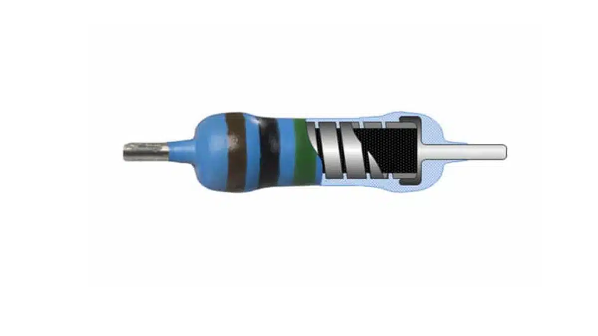
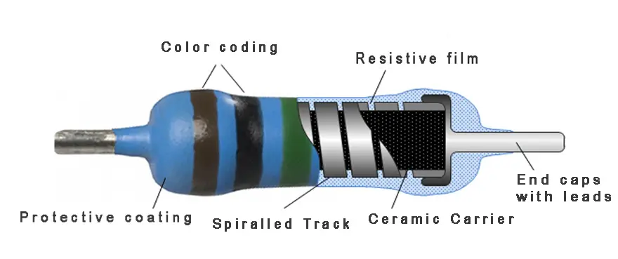
Film resistors are built either on cylindrical rods or on planar substrates. Usually the material in the rods and substrates is ceramic in the state of aluminum oxide (alumina), but glass may occur. Hollow cores exist but are more and more abandoned when sizes are becoming smaller. This design suffers also from drawbacks: the construction is more fragile and the heat dissipation is poorer than that of a solid core.
A typical through hole film resistor construction is shown in Figure 1.
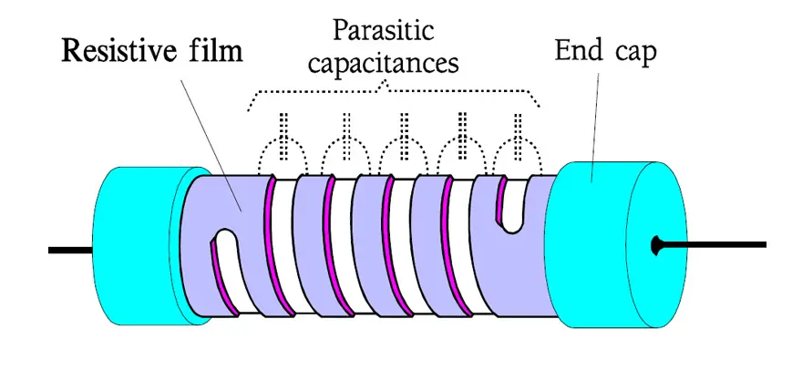
The film of the cylindrical rods thus are cut in a helical track to a long path, usually with a laser. A more stylized sketch is shown in Figure 2. The pitch of the helix track can be varied in order to increase the resistance of the film. For thick films an increase of up to 150 times, for carbon and metal films up to 1000 times or even more.
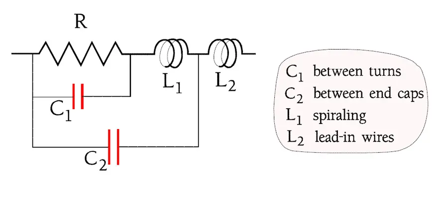
As indicated in the figure a stray capacitance is developed between the turns. Because the turns also constitute a coil the resistor will get a certain inductance. All in all the spiraling produces a frequency dependent impedance where the capacitance is dominating. The conditions are illustrated by the Figure 3.
Film resistors may be approximately classified as follows:
- values < 100Ω are inductive.
- values between 100Ω and 470Ω are practically true resistive.
- values above 470Ω are capacitive.
High‑Frequency and RF Behaviour
Spiral‑trimmed cylindrical metal film resistors exhibit measurable parasitic inductance and capacitance which limit their use at higher frequencies.
- Low‑value axial metal film parts (<100 Ω) behave mainly inductive because the helical path forms a small coil; high‑value parts (>470 Ω) show dominant capacitive behaviour between turns.
- Thin film chips with serpentine patterns have much lower parasitics; typical inductance is in the single‑digit nH range and parasitic capacitance in the low pF region.
- Bulk metal foil resistors are photo‑etched into compact serpentine or labyrinth patterns, further reducing inductance and capacitance and improving high‑frequency stability.
In practice:
- For precision analog up to ≈10–20 MHz, thin film chips and foil resistors are preferred for gain‑setting and feedback paths.
- For RF front‑ends into the hundreds of MHz and GHz, use compact thin film or foil chips with short, wide PCB pads, and avoid long spiral‑trimmed leaded parts.
- Keep lead and trace lengths minimal and avoid via‑in‑pad under precision film resistors unless controlled in the layout, to limit additional inductance and radiation.
A simple rule of thumb: select thin film chips or foil for frequency‑critical precision nodes; reserve spiral‑trimmed leaded parts for lower‑frequency, less critical positions.
SMD Chip Resistor Types
The predominant part of all chips are manufactured with thick film, but thin film chips are becoming more and more common. Also metal foil exists as SMD. The construction is like the one in Figure 4. Certain types have an organic protection in one or two layers on top of the glass passivation.
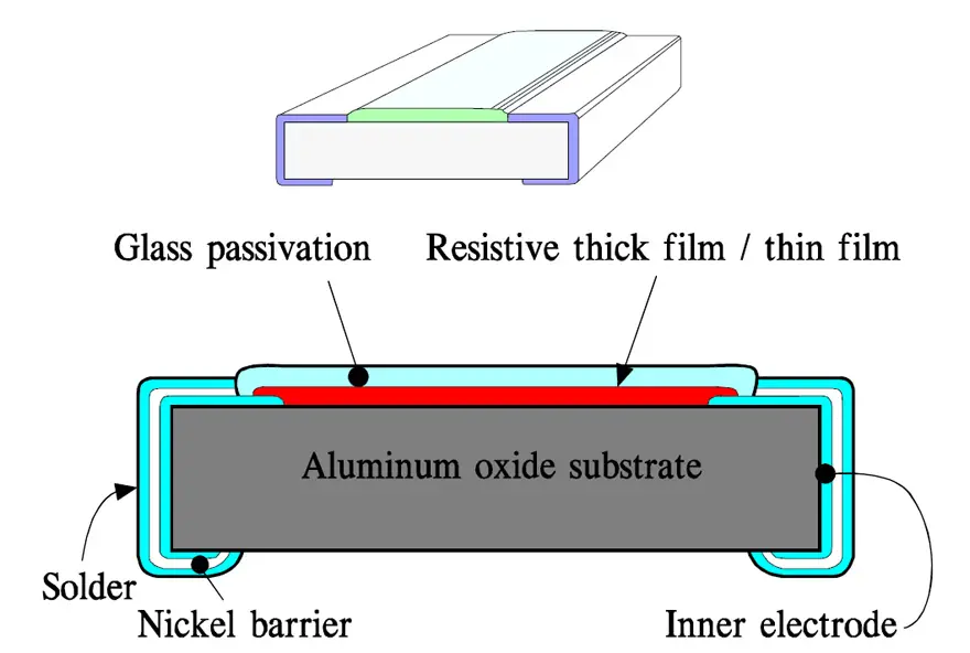
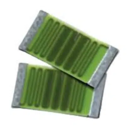
The substrates are screen printed either with a metal powder paste that is fired to a metal glaze / thick film. Or metal foils are glued on a substrate or metal films are vaporized or ion implanted on it.
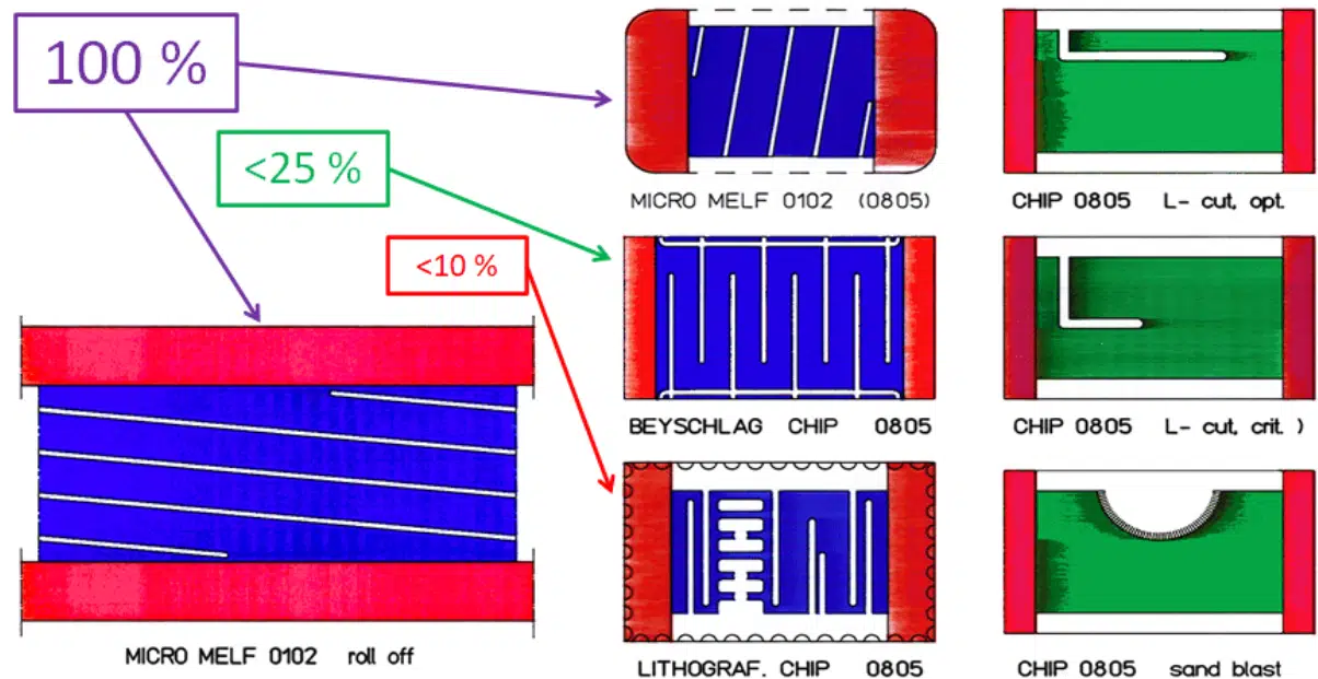
The thick film is laser trimmed to the right resistance value by cutting a track in the long side of the film. Recent manufacturing improvements however begin making this laser trimming unnecessary. This approach without any trimming tracks will increase the pulse load capability by 2 to 3 times. The other films are designed to an inductance-reducing serpentine pattern according to Figure 5. and 6.
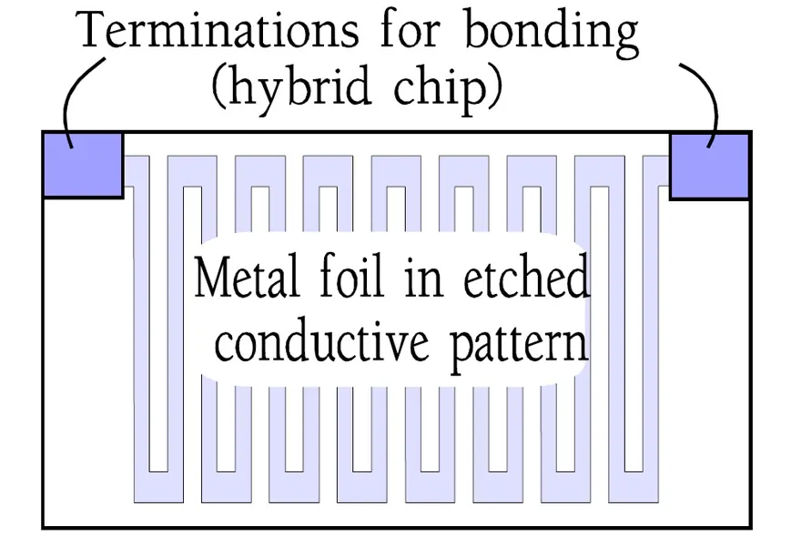
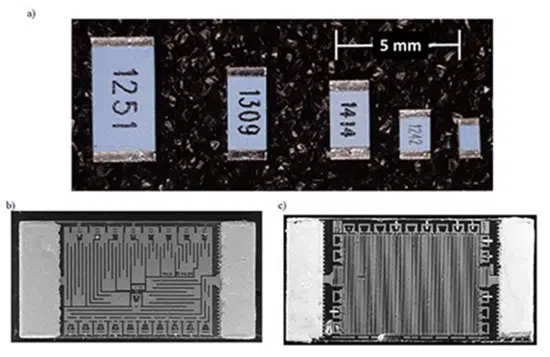
The metal foil pattern is etched chemically or patterned by means of an ion beam. The thin metal films are applied through a mask to the desired shape.
Thin Film Chip vs MELF vs Leaded Styles
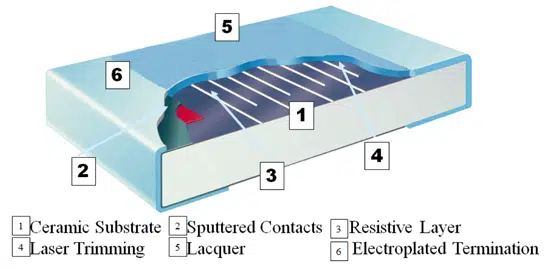

Construction Overview
| Feature | Thin film chip (SMD) | Metal film MELF | Metal film leaded (axial) |
|---|---|---|---|
| Substrate | Planar alumina chip | Cylindrical alumina body | Cylindrical alumina rod |
| Film | Sputtered metal alloy (Nichrome/TaN) | Sputtered/plated metal film | Sputtered/evaporated metal film |
| Trimming | Laser / photo‑etched pattern | Helical laser spiral or pattern | Helical laser spiral |
| Terminations | Ni barrier + Sn solder terminations | End caps + plating | Axial leads welded to end caps |
| Protection | Epoxy / passivation over film | Lacquer / molding | Lacquer / molding / sometimes hermetic |
Electrical and Application Aspects
- Thin film chips: best for automated assembly, minimal parasitics if layout is short and wide; used where compact precision is needed.
- MELF: cylindrical geometry enables longer current path and higher allowable surface load and pulse capability than equivalent chip sizes.
- Leaded metal film: convenient for through‑hole, elevated mounting, and better creepage in high‑voltage or legacy designs.
Figures 4.–6. in the source show that for the “0805 equivalent” footprint, the MELF design allows higher surface loading and better pulse endurance than thin or thick film chips.
MELF capacitors that are also available in (micro)-chip case sizes have its advantage with possible path around the whole chip that makes it more efficient compare to Thick/Thin film SMDs. See the current path example on 0805 chip equivalent in Figure 9. below and pulse load capability comparison in Figure 10.:
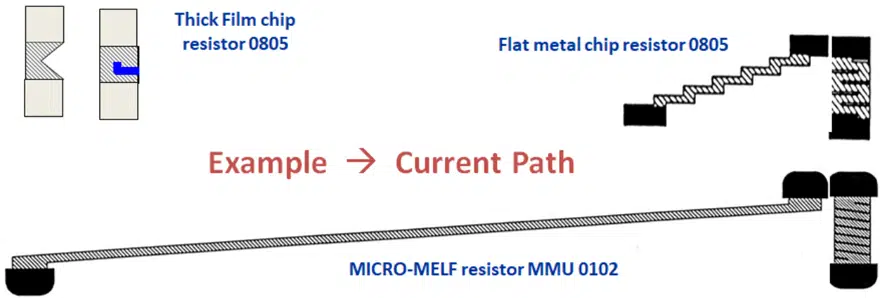
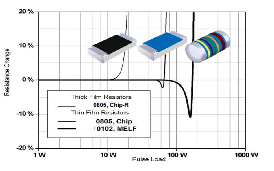
The differences in effective current length path are also reflected in the possible surface loads [W/mm2]. See the Figure 11. below.
Metal Foil Precision Resistors as a Special Case
Metal foil resistors use a relatively thick metal foil (≥2.5 µm) bonded to a ceramic substrate; the composite is designed so that thermal expansion of the foil is mechanically constrained by the substrate.
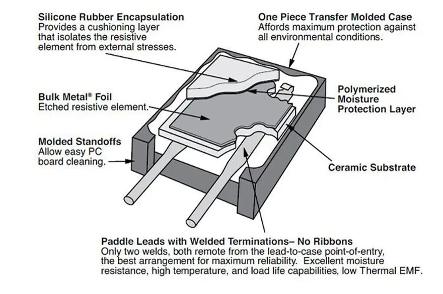
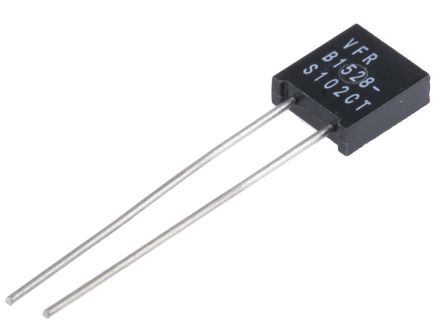
Within the metal film technology there is a particular type of precision resistor made by metal foils, by the inventor, Vishay, called Bulk metal foil. These resistors exist both in axial and radial designs for hole mount, further as SMDs, networks and power styles, finally also in PTC designs.
Figure 12. shows a principle cutaway view of a foil resistor from the manufacturer VPG foil resistors. The etching pattern is not shown.
Key points:
- TCR and stability are improved by matching foil resistivity vs temperature to the stress induced by substrate expansion, yielding very low net TCR and drift.
- The foil is photo‑etched or ion‑etched into serpentine or labyrinth patterns that minimize inductance and allow fine trimming.
- Foil thickness gives excellent pulse handling and eliminates the extreme corrosion sensitivity of ultra‑thin films.
- Maximum resistance value is limited compared with thin film, so foil is typically used at low–medium values where ultra‑precision is demanded.
Failure modes are mainly open contacts or local resistance shifts where weak spots in the foil pattern burn out.
Electrical Characteristics and Performance Ranges
Typical Parameter Ranges
The table below consolidates film‑technology ranges relevant to design.
| Parameter | Thin / metal film | Metal foil | Thick film (for comparison) |
|---|---|---|---|
| Typical resistance range | 0.2 Ω – 20 MΩ | up to a few hundred kΩ–MΩ (limited) | 1 Ω – 100 MΩ |
| Tolerance | ±0.1% – ±2% | ±0.005% – ±0.1% (vendor‑specific) | ±1% – ±5% |
| TCR | ±5 – ±50 ppm/°C | near zero to ±2–5 ppm/°C (typ.) | ±50 – ±200 ppm/°C |
| Max operating temperature | ≈155 °C | similar or higher (per datasheet) | ≈155 °C |
| Max operating voltage | ≈50 – 500 V (size‑dependent) | similar to film of same size | ≈50 – 200 V |
| Non‑linearity (3rd harmonic) | >110 dB | excellent (very low) | >50 dB |
Thin film resistors can also be configured as linear PTC devices with TCR in the +2000 to +6500 ppm/°C range.
Standards and Qualification Classes
Precision film resistors are often specified and qualified according to international standards and automotive or high‑rel requirements.
- IEC 60115 and IECQ‑CECC define performance classes, test conditions and load life requirements for fixed resistors, including thin film MELF and chip styles.
- AEC‑Q200 qualification is widely used for automotive‑grade thin film and MELF resistors; it adds vibration, mechanical shock, extended temperature and humidity tests.
- MIL‑style specifications and proprietary vendor test programmes exist for bulk metal foil and high‑rel film resistors used in aerospace and metrology.
A compact mapping of common standards to typical technologies and applications is shown below:
| Standard / programme | Typical technology | Typical application domain |
|---|---|---|
| IEC 60115 / IECQ‑CECC | Thin film MELF, thin film chips | Industrial, instrumentation, general precision |
| AEC‑Q200 | Thin / metal film chips, MELF | Automotive ECUs, sensors, powertrain |
| Vendor high‑rel / MIL | Bulk metal foil, selected thin film | Aerospace, metrology, high‑rel modules |
When selecting a precision resistor, designers should verify not only nominal electrical parameters but also the applicable qualification standard, especially for automotive, industrial and high‑rel designs.
Noise, Voltage Coefficient and Long‑Term Stability
Noise
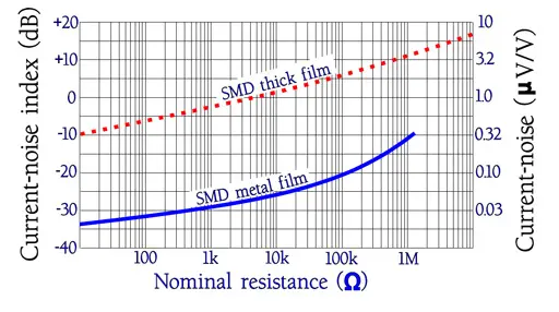
- Thin/metal film: low excess noise due to homogeneous metallic conduction; TaN films provide particularly low current noise for audio.
- Thick film: granular conduction and laser‑trim micro‑cracks cause significantly higher noise and worse 3rd‑harmonic behavior.
- Metal foil: among the quietest resistor technologies thanks to uniform foil and low trimming damage.
Figure 8. compares current noise vs resistance, clearly favoring thin film over thick film; foil is typically even better.
Voltage Coefficient and Linearity
- Helical metal films are already highly linear; remaining non‑linearity is mainly from voltage coefficient and self‑heating.
- Thick film has noticeable non‑linearity at relatively low resistances due to its complex conduction network.
- Metal foil achieves outstanding voltage coefficient and linearity by design of the foil/substrate system and serpentine pattern.
Long‑Term Stability
Failure Modes and Reliability Considerations
Film resistors fail mainly through overstress, environmental degradation or mechanical damage, not through gradual wear‑out alone.
Typical failure mechanisms include:
- Local film damage and open circuits caused by excessive pulse energy or repeated overload beyond the rated pulse curves.
- Moisture‑driven electrolytic corrosion of ultra‑thin CrNi films, especially at very high resistance values and in contaminated atmospheres.
- Mechanical cracking of the ceramic substrate or end‑caps due to PCB flex, poor support or aggressive cleaning processes.
- For foil technology, localized burn‑out of weak spots in the foil pattern under severe overload, resulting in small resistance shifts or opens.
Diagnostic signs in the lab:
- Sudden, large resistance changes after a pulse or surge event usually indicate film damage rather than normal drift.
- Gradual drift over load life tests correlates strongly with hotspot temperature and applied power; proper derating keeps drift within specified bands.
- Visual inspection can reveal end‑cap discoloration, cracked lacquer or substrate, and corrosion patterns near terminations.
Good design practice combines electrical derating with mechanical robustness and environmental protection to minimize these failure mechanisms over product life.
- Stability improves strongly when power and ambient temperature are derated relative to nominal ratings.
- IEC classes allow very tight stability (down to 0.05%) for precision thin film styles rated at lower power and temperature.
- High‑precision parts are aged during manufacture to release early drift before shipment.
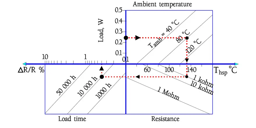
Nomographic load charts like Figure 13. relate power, hotspot temperature, ambient and resistance to expected drift; designers should verify that expected drift over life meets budget.
In general, thin film designs are providing better longer term stability, lower noise and robustness against soldering heat as shown in the following Figures 14.:
Thick vs Thin Film Summary Comparison
Thin film chip resistors achieve much better TCR and absolute resistance tolerances than thick film because of their homogeneous metallic films, controlled sputtering processes and gentle laser trimming. The higher element material density and improved heat conduction support better precision, lower electrical noise and more predictable high‑frequency behaviour.
Thick film resistors excel in cost, very wide resistance range and inherent moisture robustness, at the expense of higher noise and less linearity due to granular conduction. For short, high‑amplitude pulses in the ≈10–100 µs range, standard thick film chips can outperform ultra‑thin precision films, but thin film MELF geometries offer significantly higher destructive pulse limits than both thick and thin film chips of the same 0805 footprint.
In design terms:
- Consider MELF thin film where PCB footprint is constrained but high pulse load capability or surface power density is critical.
- Prefer thin / metal film when tolerance ≤1 %, TCR ≤50 ppm/°C, low noise and long‑term stability drive the specification.
- Prefer thick film when cost, resistance values well above tens of megohms and short‑pulse robustness are more important than ultimate precision.
Temperature, Humidity and Drift Considerations
Temperature Effects
- TCR defines reversible change with temperature; drift adds irreversible change with time and stress.
- Thin film can achieve ±5…±25 ppm/°C, but finest TCR grades often apply over a restricted temperature range.
- Linear PTC thin films use alloys with intentionally high positive TCR for sensing or compensation.
Metal oxide films can be used at much higher hotspot temperatures (up to ≈275 °C in some power types) because the film is already oxidized.
Humidity and Corrosion
- Very thin metal films (≤350 Å) are highly sensitive to moisture‑related electrolytic corrosion, especially CrNi; designers should avoid using the very highest catalogued values in harsh environments.
- Robust encapsulation (multi‑layer lacquer or hermetic sealing) substantially improves humidity performance; multi‑layer lacquers can outperform some molded plastics.
- Tantalum nitride and specially processed Nichrome thin films offer improved moisture resistance.
As a rule of thumb, avoid using values near the maximum available resistance for a given size in high‑reliability thin film designs and verify multiple suppliers’ limits.
Pulse and Overload Capability
Thin film and metal film resistors are sensitive to power pulses because the thin track heats rapidly.
- Conservative guidance: keep repetitive pulse power ≤2× rated power (PR) and avoid exceeding 4× PR even if average power is within limits; single pulses may be higher but must be checked against manufacturer’s pulse curves.
- Very low‑ohmic metal film parts historically used plated alloy layers (1–5 µm) without spiraling, with much better pulse capability but poorer tolerance and TCR; modern sputtered low‑ohm thin film improves precision but sacrifices some pulse strength.
MELF geometries permit longer current paths and higher permissible surface power density than the equivalent chip sizes; comparative curves (Figures 11–12) show MELF outperforming both thin and thick film chips for pulse load on an 0805‑equivalent footprint.
Layout and PCB Design Recommendations
For thin/metal film resistors:
- Maintain at least ≈0.5 mm clearance or insulation to adjacent conductors or metal parts to avoid arcing and local heating.
- For axial parts, consider mounting them slightly above the PCB for better cooling and creepage at higher voltages.
- Minimize loop area and lead length in precision and RF circuits to reduce inductive effects, especially with spiral‑trimmed leaded parts.
- Avoid placing precision resistors in hotspots (near power devices) and in high humidity zones (board edges, vents) unless rated and encapsulated accordingly.
- For high‑precision or high‑voltage networks, use matched resistor networks or arrays on a common substrate for tighter tracking.
When high surge or ESD exposure is expected, verify specific pulse and ESD ratings; close‑tolerance, ultra‑thin films can be more ESD‑sensitive.
Typical Applications for Thin and Metal Film Resistors
- Precision gain and reference chains in instrumentation amplifiers, ADCs, DACs and sensor front‑ends.
- Low‑noise feedback resistors in audio pre‑amps, filters and active crossovers.
- Precision RC networks for time constants and filters in communication and control systems.
- Linearity‑critical circuits (e.g. integrators, precision current sources, VCO control paths).
- High‑stability dividers for voltage references, metering and calibration instruments; foil resistors dominate at the top tier.
- Linear PTC metal film resistors as temperature sensors or compensation elements in analog paths.
Thick film and carbon technologies remain preferable where cost and high‑value range dominate over precision and low noise.
Application‑to‑Technology Mapping
| Application example | Preferred technology | Key reason |
|---|---|---|
| ADC reference divider, instrumentation amp | Thin film chip / foil | Tight tracking, low drift, low noise |
| Audio pre‑amp feedback, filters | Thin / metal film | Low current noise, good linearity |
| Metrology reference module | Bulk metal foil | Ultra‑precision, near‑zero TCR |
| Cost‑sensitive digital pull‑ups / dividers | Thick film chip | Low cost, wide resistance range |
| High‑temperature power resistor | Metal oxide film / wirewound | Hotspot capability >155 °C |
| High‑pulse surge limiter | Carbon film MELF / thick film | Superior destructive pulse loadeb:8] |
When to Prefer Thin Film over Thick Film
Practical Selection Guide
Use thin/metal film instead of thick film when:
- Tight tolerance and low TCR are required (≤1% and ≤50 ppm/°C, often better).
- Low current noise or very good linearity is essential (audio, precision analog, RF front‑end).
- Long‑term stability and low drift are important (industrial, medical, measurement equipment).
- Voltage coefficient and 3rd‑harmonic distortion must be minimized.
Use thick film instead of thin film when:
- Cost and very wide resistance range (up to 100 MΩ and more in small chips) are primary.
- Short, high‑amplitude pulses (≤100 µs range) dominate and noise/linearity are less critical.
- High‑ohmic, high‑voltage networks with good moisture robustness are needed and precision can be modest.
Key Thin vs Thick Film Chip Characteristics
| Characteristic | Thin film chip | Thick film chip |
|---|---|---|
| Film thickness | ≈0.1 µm | ≈100 µm |
| Process | Sputtering (vacuum deposition) | Screen / stencil printing |
| Tolerance | ±0.1 – ±2% | ±1 – ±5% |
| TCR | ±5 – ±50 ppm/K | ±50 – ±200 ppm/K |
| Resistance range | ≈0.2 Ω – 20 MΩ | ≈1 Ω – 100 MΩ |
| Non‑linearity | >110 dB | >50 dB |
| Noise, stability | Low noise, high stability | Higher noise, lower stability |
Conclusion
Thin film, metal film, and metal foil resistors represent the precision tier of resistor technologies, offering superior performance in tolerance, TCR, noise, and long-term stability compared to thick film alternatives. Metal foil resistors occupy the highest-precision niche with near-zero TCR and exceptional linearity, while standard thin and metal film types serve the broad range of precision analog, measurement, and low-noise applications.
Selection between thin film and thick film hinges on specific circuit requirements: choose thin film when tight tolerance, low noise, excellent stability, and minimal voltage coefficient are critical; select thick film when cost, wide resistance range, and short-pulse capability take priority. MELF geometries offer advantages in pulse handling and surface power density for equivalent footprint sizes.
Proper derating, careful PCB layout, attention to humidity exposure, and awareness of pulse limitations are essential to realizing the full potential of thin and metal film resistors in demanding applications.
FAQ: Thin Film and Metal Film Resistors
Thin film resistors use a homogeneous metallic alloy film (typically Nichrome or TaN) with thickness of approximately 0.1 µm, deposited through sputtering. They offer precision tolerances of ±0.1-±2%, TCR of ±5-±50 ppm/°C, and low noise characteristics. Thick film resistors use screen/stencil printing with film thickness of approximately 100 µm, offering tolerances of ±1-±5%, TCR of ±50-±200 ppm/°C, and are more cost-effective with wider resistance ranges.
Choose thin film resistors when you need tight tolerance (≤1%), low TCR (≤50 ppm/°C), low current noise, excellent linearity, long-term stability, and minimal voltage coefficient. They are ideal for precision analog circuits, audio applications, instrumentation amplifiers, ADC/DAC reference paths, and measurement equipment.
Ultra-Precision Applications
Metal foil resistors occupy the highest-precision niche with near-zero TCR (±2-5 ppm/°C) and exceptional linearity. They are ideal for metrology, reference circuits, voltage references, metering, calibration instruments, and applications requiring tolerances as tight as ±0.005-±0.1%. The foil thickness (≥2.5 µm) provides excellent pulse handling and eliminates corrosion sensitivity.
Construction and Performance Comparison
Thin film chips use planar alumina substrates with laser/photo-etched patterns, offering minimal parasitics for automated assembly. MELF (Metal Electrode Leadless Face) resistors have cylindrical geometry enabling longer current paths, higher surface load capability, and better pulse endurance than equivalent chip sizes. Leaded metal film resistors are convenient for through-hole mounting, elevated positioning, and better creepage in high-voltage applications.
Thin/metal film resistors offer tolerances of ±0.1% to ±2% with TCR of ±5 to ±50 ppm/°C. Metal foil resistors achieve ±0.005% to ±0.1% tolerance with near-zero to ±2-5 ppm/°C TCR. Thick film resistors typically provide ±1% to ±5% tolerance with TCR of ±50 to ±200 ppm/°C.
Moisture and Corrosion Considerations
Very thin metal films (≤350 Å) are highly sensitive to moisture-related electrolytic corrosion, especially CrNi films. Robust encapsulation using multi-layer lacquer or hermetic sealing substantially improves humidity performance. Tantalum nitride and specially processed Nichrome thin films offer improved moisture resistance. Avoid using maximum resistance values in harsh environments for high-reliability designs.
Thin film resistors are sensitive to power pulses due to rapid heating of the thin track. Conservative guidance: keep repetitive pulse power ≤2× rated power and avoid exceeding 4× rated power even if average power is within limits. MELF geometries permit higher permissible surface power density than equivalent chip sizes. Thin film handles longer pulses better, while thick film excels at short pulses (≤100 µs).
Design Best Practices
Maintain at least 0.5 mm clearance to adjacent conductors to avoid arcing and local heating. For axial parts, mount slightly above the PCB for better cooling and creepage at higher voltages. Minimize loop area and lead length in precision and RF circuits to reduce inductive effects. Avoid placing precision resistors in hotspots (near power devices) or high humidity zones unless properly rated and encapsulated.
Thin/metal film resistors cover 0.2 Ω to 20 MΩ. Metal foil resistors are typically limited to a few hundred kΩ-MΩ due to manufacturing constraints. Thick film resistors offer the widest range at 1 Ω to 100 MΩ or more, making them cost-effective for high-value applications.
TCR and Drift Characteristics
TCR defines reversible change with temperature, while drift adds irreversible change with time and stress. Thin film achieves ±5 to ±25 ppm/°C TCR, with finest grades applying over restricted temperature ranges. Stability improves significantly when power and ambient temperature are derated. High-precision parts are aged during manufacture to release early drift before shipment.
Long-term drift and PCR in bulk metal foil datasheets describe how resistance changes under sustained power and over time. Drift values (for example ±0.005 % over 2 000 hours at rated load) indicate the stability you can expect in real service. PCR specifies additional resistance change caused by self-heating at a given power level. For metrology and reference designs, choose foil parts with very low drift and PCR, and derate power so that combined drift plus PCR stays within your error budget.
How to Select the Right Film Resistor
Quick Design Checklist for Film Resistors
Before diving into detailed selection steps, verify these six key points:
Precision need: define required tolerance and TCR (e.g. ±0.1 % / ±5 ppm/°C vs ±5 % / ±200 ppm/°C).
Environment: check operating temperature, humidity, contamination and qualification requirements (IEC, AEC‑Q200, high‑rel).
Pulse profile: characterize surge, repetitive pulse and ESD exposure; compare against manufacturer pulse curves.
Package style: choose between SMD thin film, MELF, leaded metal film or foil networks based on assembly and creepage needs.
Frequency behaviour: for high‑frequency or RF nodes, favour serpentine thin film or foil with short, wide pads and minimal lead length.
Cost tier: decide whether ultra‑precision foil is justified, or whether standard thin / metal film or thick film meets the requirement.
This checklist helps narrow technology choices before detailed comparison of datasheets and vendor options.
- Define Your Circuit Requirements
Identify the key specifications needed for your application: required tolerance (±0.1% for precision, ±5% for general purpose), Temperature Coefficient of Resistance (TCR) limits, operating temperature range, resistance value range, noise requirements, and long-term stability needs. Document voltage coefficient linearity requirements and pulse/ESD exposure levels.
- Evaluate Tolerance and TCR Requirements
For tight tolerance (≤1%) and low TCR (≤50 ppm/°C), select thin film or metal film resistors. For ultra-precision (≤0.1% tolerance, ≤5 ppm/°C TCR), choose metal foil resistors. If tolerance of ±1-5% and TCR of ±50-200 ppm/°C is acceptable, thick film resistors offer cost advantages.
- Assess Noise and Linearity Needs
For low-noise applications (audio, precision analog, RF front-ends), thin film offers homogeneous metallic conduction with low excess noise. Metal foil provides the quietest performance with non-linearity >110 dB. Thick film exhibits higher noise due to granular conduction and is acceptable only when noise is not critical.
- Consider Environmental Factors
For high humidity environments, verify encapsulation quality (multi-layer lacquer or hermetic sealing). Avoid very thin films (≤350 Å) in moisture-prone areas. Tantalum nitride and processed Nichrome offer better moisture resistance. For high-temperature applications (>155°C), consider metal oxide films which can operate up to 275°C.
- Analyze Pulse and Power Requirements
For repetitive pulses, keep pulse power ≤2× rated power for thin film. MELF geometries offer superior pulse handling versus equivalent chip sizes due to longer current paths. For short high-amplitude pulses (≤100 µs), thick film performs better, except where thin film MELF is specifically rated for such pulses. Verify manufacturer pulse curves for specific conditions.
- Choose the Appropriate Package Style
Select thin film chips (SMD) for automated assembly with compact precision needs. Choose MELF for higher surface load capability and better pulse endurance in equivalent footprints. Use leaded metal film for through-hole mounting, elevated positioning, and better creepage in high-voltage designs.
- Plan PCB Layout for Optimal Performance
Maintain ≥0.5 mm clearance to adjacent conductors. Mount axial parts slightly above PCB for better cooling. Minimize loop area and lead length in precision circuits. Avoid hotspots near power devices and high humidity zones (board edges, vents). Use matched resistor networks on common substrates for high-precision applications.
- Apply Proper Derating Guidelines
Derate power and operating temperature relative to nominal ratings to improve long-term stability. Use nomographic load charts to relate power, hotspot temperature, ambient conditions, and resistance to expected drift. Verify that expected drift over product lifetime meets your stability budget.
- Verify Cost-Performance Tradeoffs
Metal foil resistors provide highest precision but at premium cost and limited resistance range. Standard thin/metal film covers mainstream precision needs at moderate cost. Thick film remains the low-cost workhorse where precision is not critical, offering widest resistance range up to 100 MΩ+.
- Validate Selection with Application Testing
Confirm performance through prototype testing under actual operating conditions. Monitor drift over temperature cycling, verify noise performance in circuit, check pulse response, and validate long-term stability. Compare multiple vendors’ specifications to ensure reliability and availability.
References and Further Reading
- Thick Film and Thin Film Resistors – A Comparison – overview of thick vs thin film technology, processes and characteristic differences.
- Pulse Load on SMD Resistors: At the Limit – detailed discussion of pulse stress behaviour for chip and MELF resistors.
- Carbon Film MELF – Pulse Load Champion – analysis of carbon film MELF pulse capability versus thick and thin film chip resistors.
- Professional Thin Film MELF Resistors – product and design information for thin film MELF series in precision and automotive applications.
- Bulk Metal Foil Resistors – Design and Selector Guide – high-precision foil resistor portfolio, including drift and PCR specifications.
- Resistor Noise, Linearity and Voltage Coefficient – background on current noise, voltage coefficient and distortion in different resistor technologies.