







Passive Components Blog
No Result
View All Result
  • Home
  • News
    • All
    • Aerospace & Defence
    • Antenna
    • Applications
    • Automotive
    • Capacitors
    • Circuit Protection Devices
    • electro-mechanical news
    • Filters
    • Fuses
    • Inductors
    • Industrial
    • Integrated Passives
    • inter-connect news
    • Market & Supply Chain
    • Market Insights
    • Medical
    • Modelling and Simulation
    • New Materials & Supply
    • New Technologies
    • Non-linear Passives
    • Optoelectronics and Isolation
    • Oscillators
    • Passive Sensors News
    • Resistors
    • RF & Microwave
    • Telecommunication
    • Weekly Digest
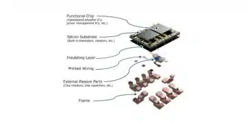
    Exploded view of the Nisshinbo Silicon Motherboard: functional chip, silicon substrate, insulating layer, printed wiring, external passive parts and frame

    Nisshinbo Silicon Motherboard Integrates ICs and Passives

    Murata MGJ2T2 SIP isolated DC-DC converter for SiC gate-drive power

    Murata Unveils Isolated DC-DC for SiC Gate Drives

    Simplified buck, boost, flyback and isolated buck power-stage schematics showing switches, inductors, coupled magnetics, diodes and output capacitors.

    SMPS Topology Selection: From Buck and Boost to Flyback and LLC

    Littelfuse AK-FB and AK-A high-power TVS diodes in axial-leaded packages

    Littelfuse Introduces TVS Diodes for HVDC Protection

    Wk 46 Electronics Supply Chain Digest

    VACUUMSCHMELZE VACODUR Max cobalt-iron lamination material illustrated as thin metallic rotor and stator stacks.

    VACUUMSCHMELZE Introduced VACODUR Max Cobalt-Iron Alloy for Motor Laminations

    Stackpole RPCQ thick-film chip resistors in rectangular surface-mount packages with end terminations

    Stackpole Releases Pulse-Withstanding Chip Resistors up to 4 W

    Bourns CRT-G thin film chip resistor illustration with a rectangular body and metallic end terminations

    Bourns Introduces Precision Thin Film Resistors for Measurement

    Würth Elektronik ABC of Thermal Management textbook

    Würth Elektronik Launches ABC of Thermal Management Guide

    Trending Tags

    • Ripple Current
    • RF
    • Leakage Current
    • Tantalum vs Ceramic
    • Snubber
    • Low ESR
    • Feedthrough
    • Derating
    • Dielectric Constant
    • New Products
    • Market Reports
  • Knowledge Blog
  • Dossiers
    • Aerospace and Defense Passive Components Dossier
    • AI Hardware Dossier
    • Automotive Dossier
    • Industrial Robotics Dossier
    • Power Converter Dossier
    • Capacitor Dossier
    • Circuit Protection Dossier
    • Inductor Dossier
    • Resistor Dossier
    • Silicon Capacitors and Integrated Passives Dossier
  • Suppliers
    • Who is Who
  • PCNS
    • PCNS 2025
    • PCNS 2023
    • PCNS 2021
    • PCNS 2019
    • PCNS 2017
  • Events
  • Home
  • News
    • All
    • Aerospace & Defence
    • Antenna
    • Applications
    • Automotive
    • Capacitors
    • Circuit Protection Devices
    • electro-mechanical news
    • Filters
    • Fuses
    • Inductors
    • Industrial
    • Integrated Passives
    • inter-connect news
    • Market & Supply Chain
    • Market Insights
    • Medical
    • Modelling and Simulation
    • New Materials & Supply
    • New Technologies
    • Non-linear Passives
    • Optoelectronics and Isolation
    • Oscillators
    • Passive Sensors News
    • Resistors
    • RF & Microwave
    • Telecommunication
    • Weekly Digest
    Exploded view of the Nisshinbo Silicon Motherboard: functional chip, silicon substrate, insulating layer, printed wiring, external passive parts and frame

    Nisshinbo Silicon Motherboard Integrates ICs and Passives

    Murata MGJ2T2 SIP isolated DC-DC converter for SiC gate-drive power

    Murata Unveils Isolated DC-DC for SiC Gate Drives

    Simplified buck, boost, flyback and isolated buck power-stage schematics showing switches, inductors, coupled magnetics, diodes and output capacitors.

    SMPS Topology Selection: From Buck and Boost to Flyback and LLC

    Littelfuse AK-FB and AK-A high-power TVS diodes in axial-leaded packages

    Littelfuse Introduces TVS Diodes for HVDC Protection

    Wk 46 Electronics Supply Chain Digest

    VACUUMSCHMELZE VACODUR Max cobalt-iron lamination material illustrated as thin metallic rotor and stator stacks.

    VACUUMSCHMELZE Introduced VACODUR Max Cobalt-Iron Alloy for Motor Laminations

    Stackpole RPCQ thick-film chip resistors in rectangular surface-mount packages with end terminations

    Stackpole Releases Pulse-Withstanding Chip Resistors up to 4 W

    Bourns CRT-G thin film chip resistor illustration with a rectangular body and metallic end terminations

    Bourns Introduces Precision Thin Film Resistors for Measurement

    Würth Elektronik ABC of Thermal Management textbook

    Würth Elektronik Launches ABC of Thermal Management Guide

    Trending Tags

    • Ripple Current
    • RF
    • Leakage Current
    • Tantalum vs Ceramic
    • Snubber
    • Low ESR
    • Feedthrough
    • Derating
    • Dielectric Constant
    • New Products
    • Market Reports
  • Knowledge Blog
  • Dossiers
    • Aerospace and Defense Passive Components Dossier
    • AI Hardware Dossier
    • Automotive Dossier
    • Industrial Robotics Dossier
    • Power Converter Dossier
    • Capacitor Dossier
    • Circuit Protection Dossier
    • Inductor Dossier
    • Resistor Dossier
    • Silicon Capacitors and Integrated Passives Dossier
  • Suppliers
    • Who is Who
  • PCNS
    • PCNS 2025
    • PCNS 2023
    • PCNS 2021
    • PCNS 2019
    • PCNS 2017
  • Events
No Result
View All Result
Passive Components Blog
No Result
View All Result

Researchers Measure How Specific Atoms Move In Dielectric Materials

23.10.2015
Reading Time: 3 mins read
A A

source: ECN article

Thu, 10/01/2015 – 9:24am by North Carolina State University

RelatedPosts

Nisshinbo Silicon Motherboard Integrates ICs and Passives

Murata Unveils Isolated DC-DC for SiC Gate Drives

SMPS Topology Selection: From Buck and Boost to Flyback and LLC

Researchers have measured how the atoms within electrically insulating solids reorient due to an applied electric field. Shown here for Na1/2Bi1/2TiO3, bismuth ions (purple) align along the electric field direction relative to their surrounding titanium ions (blue). Oxygen ions not shown. Credit Tedi-Marie Usher

Researchers from North Carolina State University, the National Institute of Standards and Technology (NIST), and UNSW Australia have measured the behavior of specific atoms in dielectric materials when exposed to an electric field. The work advances our understanding of dielectric materials, which are used in a wide variety of applications – from handheld electronics to defibrillators.

“Dielectric materials are insulators that can store and manage electric charge. But we hadn’t yet directly measured how atoms move in dielectric materials in order to store that charge,” says Tedi-Marie Usher, a Ph.D. candidate in materials science and engineering at NC State and lead author of a paper on the work.

To get to the bottom of this problem, the researchers applied voltage to a dielectric material, creating an electric field. They simultaneously bombarded the material with X-rays from a synchrotron at Argonne National Laboratory’s Advanced Photon Source. When the X-rays hit the material, they scatter into a pattern of bright rings. Typically, to figure out the arrangement of atoms in a material, the positions and intensities of these bright rings are analyzed.

However, by applying new mathematical techniques that are more sensitive to the weak (dim) scattered X-rays, the researchers could determine changes in the placement of specific atoms within the crystalline structure of the material. In other words, the researchers could “see” how the atoms moved relative to each other in response to the electric field.

“A good analogy would be that analyzing the bright rings is like examining a skyscraper from far away and determining that each office is 500 square feet. However, by also analyzing the weak X-rays scattered from the sample, we can determine that some offices are 400 square feet and others are 600 square feet, and some have the desk on the east side, and others have the desk on the north side,” says Usher. This is an uncommon approach, because experimenters typically only evaluate the bright rings.

“What’s really new here is that this technique is much more sensitive to the behavior of select atoms relative to their neighboring atoms, rather than looking at an average of all the atoms in a sample,” says Jacob Jones, a professor of materials science and engineering at NC State and corresponding author of the paper.

The work uses a technique called a pair distribution function, which allows researchers to extract information about how atoms are arranged at extremely small length-scales based on the weak intensity X-rays diffracted from a sample. The researchers evaluated three different dielectric materials for this study.

“One of the interesting findings here is that each of the three dielectric materials we tested exhibited very different behaviors at the atomic level – there was no single atomic behavior that accounted for dielectric properties across the materials,” Jones says.

For example, the researchers tested a material called sodium bismuth titanate – a non-toxic material that is thought to be promising for use in dielectric devices. In the absence of an electric field, researchers knew that the bismuth ions are off-center relative to neighboring atoms. But different bismuth ions would be off-center in different directions. However, when an electric field is applied, virtually all of the bismuth ions shifted so they were off-center in the same direction as the electric field.

“Neither of the other dielectric materials exhibited similar behavior,” Usher says. “One of our questions for future work is whether the bismuth behavior we saw in sodium bismuth titanate is consistent across bismuth-based dielectrics.”

“We also want to know how dielectric materials and other complex materials, such as high-entropy alloys, behave at the atomic scale when under mechanical stress,” Jones says.

Source: http://www.eurekalert.org/pub_releases/2015-10/ncsu-rmh092915.php

Related

Recent Posts

Simplified buck, boost, flyback and isolated buck power-stage schematics showing switches, inductors, coupled magnetics, diodes and output capacitors.

SMPS Topology Selection: From Buck and Boost to Flyback and LLC

16.11.2026
8
VACUUMSCHMELZE VACODUR Max cobalt-iron lamination material illustrated as thin metallic rotor and stator stacks.

VACUUMSCHMELZE Introduced VACODUR Max Cobalt-Iron Alloy for Motor Laminations

12.11.2026
74
Schematic of six-arm nitrene crosslinker joining PEI polymer chains in a free-standing dielectric film.

Crosslinked PEI Film Capacitor Dielectrics Reach 6 J/cm³ at 200°C

11.11.2026
32
Conceptual illustration of Peak Nano NanoPlex HDC capacitor dielectric film rolls beside a cast-film production line

Peak Nano Scales NanoPlex HDC Capacitor Film Production 20-Fold

10.11.2026
35
Reference tantalum capacitor anode characterization, tantalum anode modeling, process selection and life-test verification.

Tantalum Anode Design Combines Structural Benchmarks and Modeling

9.11.2026
29
Illustration of a thin-film capacitor stack with TiN electrodes and an ultrathin hafnium zirconium oxide ferroelectric layer on silicon

Sub-Volt Ferroelectric HZO Capacitor Pairs Speed and Endurance

6.11.2026
27
Cut-open lithium-ion capacitor pouch cell showing stacked carbon electrodes and separators, with vials of carbon powder

Lithium-Ion Capacitor Review Backs Hard Carbon//AC Pairing

6.11.2026
27
Rack power shelf in an AI data center with film DC-link capacitors, a supercapacitor bank and a converter board

800 VDC AI Data Centers Reshape Capacitor Demand for 2027

6.11.2026
116
Conceptual polypropylene DC-link film capacitor module with parallel cells and copper interconnections

DC-Link Film Capacitor Modules: Inductance and Thermal Design, Jianghai-Europe Tech Memo

3.11.2026
49

Upcoming Events

Nov 24
16:00 - 17:00 CET

Select the Correct Components for Your DC/DC Converter

Dec 1
16:00 - 17:00 CET

Developing low-noise mixed-signal systems

Dec 8
16:00 - 17:00 CET

WE-CCMF: Design Principles, Layout Guidelines and Measurement Results for High-Speed EMI Filtering

View Calendar

Popular Posts

  • Buck Converter Design and Calculation

    0 shares
    Share 0 Tweet 0
  • September 2026 Interconnect, Passives and Electromechanical Components Market Insights

    0 shares
    Share 0 Tweet 0
  • Boost Converter Design and Calculation

    0 shares
    Share 0 Tweet 0
  • Capacitor Charging and Discharging

    0 shares
    Share 0 Tweet 0
  • LLC Resonant Converter Design and Calculation

    0 shares
    Share 0 Tweet 0
  • RF Connector Types: How To Choose the Right One

    0 shares
    Share 0 Tweet 0
  • Passive Low Pass Filters: Fundamentals and EMI Design

    0 shares
    Share 0 Tweet 0
  • Flyback Converter Design and Calculation

    0 shares
    Share 0 Tweet 0
  • MLCC and Ceramic Capacitors

    0 shares
    Share 0 Tweet 0
  • Capacitor Symbols

    0 shares
    Share 0 Tweet 0

Newsletter Subscription


Passive Components Blog

© 2015–2026
All rights reserved

  • Home
  • Privacy Policy
  • EPCI Membership & Advertisement
  • About

No Result
View All Result
  • Home
  • Knowledge Blog
  • Dossiers
  • PCNS

© 2015–2026
All rights reserved