In this comprehensive guide to filters and RF inductors we explore passive filter fundamentals including capacitors and resistors, then delve into EMI and RF inductors with advanced selection methodologies for modern high-frequency applications.
As wireless systems evolve toward 5G/6G, Wi-Fi 6E/7, and millimeter-wave frequencies, understanding RF inductor selection, parasitic management, and technology trade-offs has become essential for achieving optimal performance in demanding RF circuits
This article provides a practical overview of passive RF filters and RF inductors from an EMC and RF front‑end perspective. It connects basic LC/RC filter concepts with real‑world EMI/RFI filters, LTCC‑based RF components and discrete RF inductors used in modern communication systems. For a deeper mathematical treatment of low‑pass filters, see the article What Electronics Engineer Needs to Know About Passive Low Pass Filters, and for general inductor basics see What is an Inductor?.
Key Takeaways
- Passive filters and RF inductors work together to control frequency response, attenuation and EMC performance in RF and power electronic systems.
- LTCC and SMD technologies enable compact, high‑frequency filters, baluns, antennas and RF inductors with well‑controlled parasitics and high reproducibility.
- RF inductors differ from power inductors by prioritising SRF, Q‑factor and impedance control over current handling, making correct technology and value selection critical for RF filters, matching networks and low‑noise front‑ends.
- Proper selection, PCB layout and derating of RF inductors and EMI filters are essential to achieve reliable operation and compliance with EMC and automotive standards such as AEC‑Q200 and MIL‑STD‑220.
- Self-Resonant Frequency (SRF) should be at least 10× the operating frequency to maintain predictable inductive behavior and avoid circuit instability
- Technology selection (wire-wound, multilayer ceramic, thin-film, air-core) involves critical trade-offs between Q-factor, size, current handling, and cost
- Accurate simulation models, VNA verification with proper calibration, and tolerance management are essential for first-pass design success
- Plating materials (gold vs. tin), core materials, and physical construction significantly impact performance, with gold plating offering 10-30% Q improvement above 5 GHz
The article is split into following chapters:
- Filters Basic Concepts
- Filter Construction
- LTCC Components and RF inductors
Read more about RF inductors key characteristics and applications in article here: RF Inductors Key Characteristics and Applications
Filters Basic Concepts
Filters that contains one or more capacitor elements with paper, plastic film or ceramic dielectric combined with one or more inductive elements in the form of ferrites or chokes are called LC filters. Ceramic capacitors used are of feed-through type, where one terminal consist of the casing that is soldered or screwed to the chassis. Or there are SMD variants.
It should also be mentioned that there are RC filters where an metallized paper (MP) capacitor is combined with a series resistance. Often the resistor element consist of a metallization alloy with higher resistivity. RC filters are mainly used for arc suppression purposes.
Some abbreviations

- RF = radio frequency = frequencies where radiation starts to appear
- RFI = radio frequency interference = induced radio frequent interference signals
- EMI = electromagnetic interference
- I.L. = Insertion Loss
- A = Attenuation
Measurements and Concepts
A filter should eliminate interference signals but transmit effective capacity and signal currents. Normally the interference signals are located in the RF range and the true signal/power currents in the low frequency range. Thus the filter should transmit low frequency signals and suppress those of higher frequencies. We call this the low-pass filter. There are, however, also other filter types as shown in Figure 1.
The common low pass filter can be described in Figure 2.
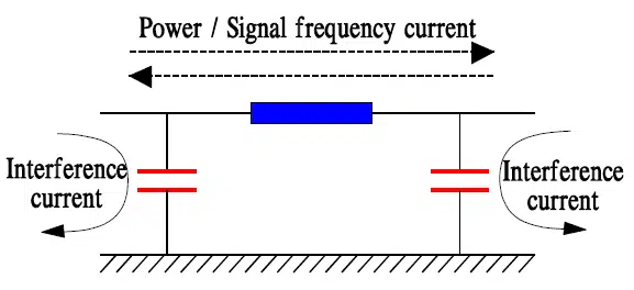
The figure shows how the interference currents are blocked by an inductor and lead away to earth via capacitors. Thus following filter concepts mainly applies to interference signals and interference frequencies.
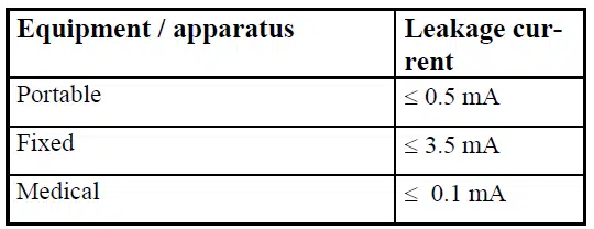
There is, however, an important exception. Filters connected between phase and earth in the mains contain those Y safety capacitors. Through them will flow a weak current at the net frequency. It is called leakage current and has to be limited to certain values. The following table 1. shows some generally accepted limits.
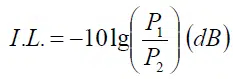
Attenuation
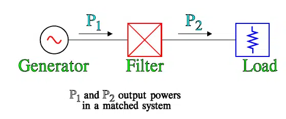
The attenuation, A, is expressed in dB and is determined in a matched system, i.e., where generator, line, filter and load have the same impedance, as a rule 50Ω.
In the system there is no reflection either from the filter or from the load. Then the attenuation A is defined as in eq.[1]:
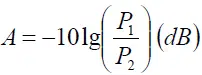
Often the minus sign is left out when we speak of attenuation.
Insertion loss, I.L.
It is very seldom that a filter is matched to the system. Then, in a strict sense of specification, we don’t speak of attenuation but of insertion loss, abbreviated I.L.
P1 represents the output power without a filter and P2 the output power from an inserted filter. The difference includes both specified attenuation and return losses. Less formally the expression attenuation is used as a measure of the signal reduction of the filter, irrespective of circuit conditions.
MIL-STD-220 defines I.L. as:
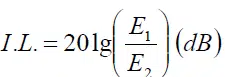
where the voltages before and after filter insertion are illustrated
in right Figure 4.
If we apply a load in the circuit that differs from the line impedance, the I. L. will be changed. The attenuation of the filter in its turn depends among other things on the DC current. Maximum DC current – full load operation – impairs inductor inductance. The attenuation decreases. Note therefore in catalogues and specifications if the I.L. concerns No load or Full load values.
If the attenuation characteristics are to be correctly established it is important that the generator side is effectively shielded from the receiver side. Moreover it is necessary to use shielded cables, correct connectors and test fixtures supplied with shielding walls.
The manufacturer’s data over I.L. is a guidance. In the practical circuit, however, the attenuation generally is poorer.
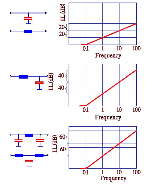
Filter Types and Their Mounting
The LC filters are built up by their elements in certain basic configurations. In the following sequence of figures it is shown which basic style that has to be used in different impedance conditions in order to reduce the mismatch.
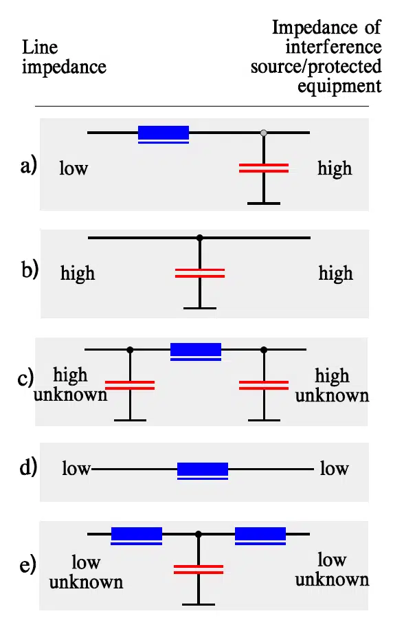
Filter types:
a) = L
b) = C
c) = π
e) = T
Theoretically, these filter styles have insertion
losses as shown in Figure 6. below:
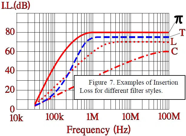
The next Figure 7. shows some examples of how the same basic elements added together in different configurations influence the attenuation in practical filters. All attenuation curves usually start leveling out at approximately 70 – 80 dB. Further attenuation is prevented by inductance and series resistance in the capacitor elements and parasitic capacitance and resistances in the inductor elements. A general recommended filter topology depending to source and load impedance requirements is shown in Figure 8.

Overview of Filter and RF Inductor Types
The main passive components discussed in this article can be summarised as follows:
| Component type | Technology / form | Typical frequency range | Main use case |
|---|---|---|---|
| Air‑core RF inductor | Wire wound on air or ceramic former | High VHF to several GHz | Matching networks, resonant tanks, RF chokes where high Q is needed |
| Multilayer ceramic RF inductor | Printed spiral in ceramic multilayer | Up to several GHz | Compact RF filters and impedance matching in mobile and wireless modules |
| Ferrite‑core RF choke | Wire wound on ferrite core | kHz to low GHz | EMI suppression and bias chokes on supply and control lines |
| LTCC low‑pass / band‑pass filter | Integrated L and C in LTCC | ~0.9 to 6 GHz | Front‑end filtering in wireless communication systems |
| Integrated EMI filter (X2Y, arrays) | Multi‑terminal MLCC / LTCC arrays | MHz to several hundred MHz | Differential and common‑mode EMI suppression with reduced parasitics |
| Discoidal / feedthrough EMI filter | Ceramic discoidals in metal housing | Wideband RF | Feedthrough filtering in connectors, bulkheads and power line filters |
RF Inductor Fundamentals: Physics and Frequency Effects
Electromagnetic Principles
RF inductors operate on Faraday’s Law of electromagnetic induction, where a time-varying current through a conductor generates a magnetic field that opposes changes in current flow. The inductance L (measured in henries) quantifies this opposition and is determined by the coil geometry, number of turns, core material permeability, and physical dimensions.
At RF and microwave frequencies, several physical phenomena that are negligible at lower frequencies become dominant:
- Skin Effect: At high frequencies, current density concentrates near the conductor surface rather than distributing uniformly across the cross-section. The skin depth δ decreases with frequency (δ ∝ 1/√f), increasing effective resistance. For copper at 1 GHz, skin depth is approximately 2 μm, making conductor geometry and surface treatment critical.
- Proximity Effect: In multi-turn inductors, magnetic fields from adjacent turns cause non-uniform current distribution, further increasing AC resistance beyond skin effect alone.
- Wavelength Considerations: When operating frequencies approach where the component dimensions become a significant fraction of the wavelength (λ = c/f), distributed effects replace lumped-element behavior. At 10 GHz in free space, λ ≈ 30 mm, making even small inductors electrically significant.
Parasitic Elements and Quality Factor
Real RF inductors exhibit parasitic resistance and capacitance that create frequency-dependent behavior:
- Equivalent Series Resistance (ESR): Combines DC resistance, skin effect losses, core losses, and radiation resistance. ESR increases with frequency due to skin and proximity effects.
- Self-Capacitance (Cp): Inter-turn and inter-layer capacitance creates a parallel resonance at the Self-Resonant Frequency (SRF). Above SRF, the component behaves capacitively rather than inductively.
The quality factor Q = ωL/ESR quantifies inductor efficiency, with higher Q indicating lower losses. At RF frequencies, achieving Q > 30 requires careful material selection and geometric optimization.
Filter Construction
HF / π / EMI / RFI filters
This type of LC filter consists in its most simple design of elements arranged as in Figure 5a or 5b. The most common types look like the one in Figure 5c. They have a feed-through design, i. e., the capacitor elements are connected direct to earth when the plated outside of the filters is soldered to the housing wall. A typical design of an EMI filter of the p type is shown in next Figure 9.
Usually the π filters are supplied with a collar that is soldered to the silvered surface (Figure 10.).

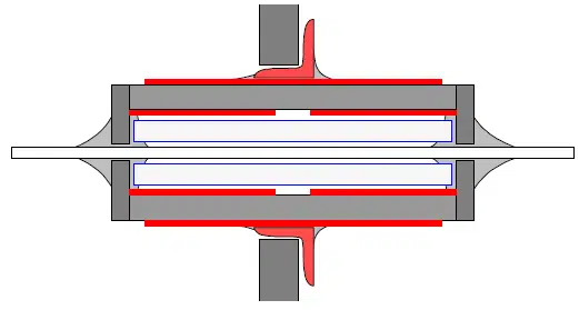
Note! If the collar in the filter in Figure 10. is soldered with a high temperature solder, check carefully that there is no unintentional solder on the top side of the collar. This would increases the outer diameter of the bushing so it will not fit in the intended hole.
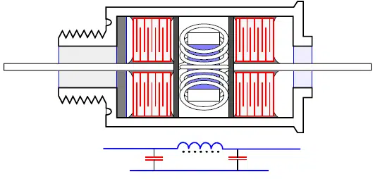
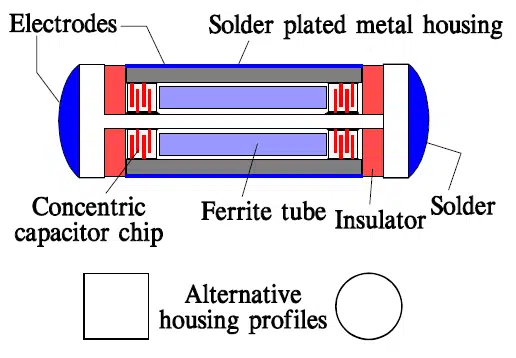
EMI filters often are sealed in metal housings that are encapsulated hermetically (Figure 11.) or by epoxy encapsulation. The capacitor elements consist of concentric chips, so called discoidals, that are soldered to the metal housing. The cases are supplied with a threaded part. More powerful filters often are supplied with a toroidal choke. They usually are built in π, L or T configurations. The stated capacitance value many times is a minimum
value, sometimes abbreviated as GMV, i.e., guaranteed min value, because it is the specified minimum attenuation that is of interest.
Failure modes
The discoidal design should be preferred to the ceramic tube design. The thin ceramic tube is brittle and has to be protected against mechanical damage and temperature gradients at the soldering. A treacherous source of errors may appear at the soldering moment. If, for example, in Figure
9. or 10. the right part of the lead-through wire is soldered and the solder heat happens to melt the seal solder around the filter inlet, the filter will be anchored in the lead-through wire only to its left solder joint.
If we then touch the right part of the lead-through wire – and this will happen during the soldering – we get a bending moment that is transferred to the ceramic tube in its fixed position to the wall. Usually it cracks. If we run the risk of melting internal solder joints we should specify high temperature solder for internal construction. The melting point usually is in the vicinity of 300 °C.
For hermetic EMI filters short-circuiting in a capacitor element is the most common. Often it is a matter of cracks in the ceramic that have cleared the way for migration of electrode metals or flux contaminants and a subsequent breakdown. Open circuit may occur and depends usually on poor internal solder joints.
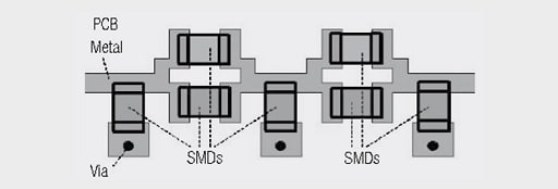
SMD designs
Figure 12. shows a construction sketch of a section through a π filter chip.
Simpler variants of π filter chips have the same buildup as the filter in Figure 8. Other designs utilize a multi-layer technique for both the capacitor and the ferrite elements. The most simple design has a T-circuit configuration with two ferrites and one capacitor connected to the ground terminal.
Integrated EMI filters
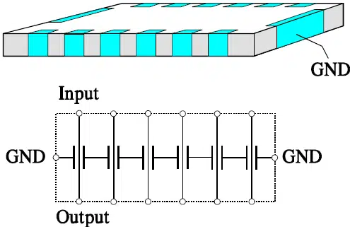
If we by means of multilayer technology build a number of ceramic capacitor elements into a ceramic block in a planar array construction we may save a considerable board space (see more in next LTCC filters chapter). Moreover, we will increase the electrical filtering capability due to reduced inductance in shorter internal conductors. This type of capacitor arrays is preferably used in EMI suppression applications. An example of such a design is shown in Figure 13.
Filters in connectors are constructed in the same way but in shape of circular discs with discoidals arranged around the pin feedthroughs. Electrical connections are through via and edge terminations.
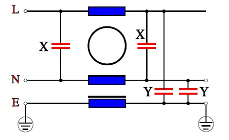
Another EMI filter, also consisting of integrated ceramic capacitors, is built of a matched and balanced pair of Y capacitors (line to ground) together with an X capacitor (between the lines) connected to a four-terminal device4 as shown in Figure 14. The device is called X2Y.
A principle sketch of the construction looks like as shown in Figure 15.


X and Y capacitors in an X2Y device reflect the patented design shown in Figure 15. These EMI filters are mostly used in lower voltage applications but larger sized X2Y devices can be designed also for mains applications where they for safety reasons require test voltages far above 1 kV.
The EMI filter X2Y has many advantages. The inserted ground planes reduce the current loop in comparison to standard MLCCs thus decreasing the inductance of the device. A further inductance reduction is achieved by the opposite current direction in opposed electrodes that is possible by the inserted ground planes. All these measures mean more effective filtering at higher frequencies.
In our Figure 15. above only two electrodes and three ground planes are shown. In practice the number of electrodes and intervened dielectric layers may be much greater, depending on the intended capacitance. The EMI filter X2Y is produced in sizes 0603 to 1812. Rated voltages for the Y capacitor elements in NP0 dielectric are 100V, in X7R dielectric 10 to 100V and in Y5V dielectric 16V. Rated voltages for X capacitors are correspondingly greater. The capacitance ranges from 10 pF in NP0 to 10mF in Y5V dielectric. Apart from the above mentioned advantages the design offers a size reduction in comparison to discrete MLCCs by integration of three capacitors in one device.
Power Line Filters
These filters often are supplied with toroidal chokes and usually have considerably more elements than in the simple π filter.
LTCC RF Filters and Passive Components
The use of LTCC (Low Temperature Co-fired Ceramic) material is gaining importance in applications in the field of communications. This is a multi-layer process used for the production of sophisticated HF components with good performance characteristics. The ceramic-based LTCC technology is an inexpensive substrate technology with which up to 50 layers are stacked on top of each other. The silver or gold conductor tracks are impressed on the “green” ceramic foil once the holes for the through contacts have been laser or mechanically generated. The various layers are then collected together and are pressed in a pressure chamber. Following lamination, the stack is sintered in a furnace, i.e. burned together at around +850 °C in process furnaces.
LTCC can be used to produce multi-layer modules in which cavities, Rs, Ls and Cs are integrated. Good thermal conductivity and a low TCE (Temperature Coefficient of Expansion) are achieved. The components are hermetically sealed, i.e. are stable against mechanical and thermal stress. The dielectric properties (εr, tanδ, the thickness) can be controlled very effectively. In addition to low‑pass and band‑pass filters, LTCC technology also enables the integration of RF inductors directly into multilayer structures. These integrated inductors exhibit low parasitics and very good reproducibility, and they form the building blocks of many LTCC filters, baluns and matching networks used in compact RF modules.


The main advantage of this technology is the high degree of miniaturisation and the ever-lower space requirement associated with it. This is illustrated by the following simple example. Rather than discreetly constructing a low-pass filter, there is the option of integrating the inductance and capacitance, e.g. as package type 0603. The integration is an important aspect in the field of RF applications.
Low-Pass Filter
HF components based on LTCC technology are designed for use in various frequency bands from around 900 MHz to 6 GHz. Application areas for these components are, for example, Wireless LAN, Bluetooth®, HomeRF, GPS, PCS, GSM, DECT and PHS.
The high precision LTCC technology gives rise to low-loss RF components with reproducible, guaranteed properties and a low space requirement.
LPF low-pass filters for diverse applications are produced in the package types 0603 to 0805. The limit frequencies of these compact low-pass filters range form 900 MHz to 5.5 GHz. The insertion loss of the low-pass filter in the admission range is very low. The low-pass filters show comparably high attenuation in the blocked range.
Band-Pass Filter BPF
The smallest band-pass filter package type is 0805. A high level of attenuation is achieved over a very wide blocking range. The insertion loss in the admittance range is very low at approx. 2 dB, however somewhat higher than the insertion loss of low-pass filters.
The example of the band-pass filter for Bluetooth® serves to illustrate where attention should be paid in the selection of components. (Figure 20.)
To effectively suppress frequencies in the mobile phone range, the attenuation in the range from 900 MHz (GSM900) to 2.1 GHz should be as high as possible. The attenuation in the WLAN/HyperLAN range should also be high. For this reason, specific poles have been placed at these frequencies for the above filter.
Balun BAL
Symmetry transformers (baluns) with low insertion loss, as well as low amplitude and phase differences, can be achieved in LTCC technology. The asymmetrical (unbalanced) impedance is 50 Ω, the symmetrical (balanced) impedance can be 50 Ω, 100 Ω or 200 Ω. Two types of baluns are distinguished: LC type and Marchand type. In the case of the latter, no DC bias may be applied. It is recommended to connect a capacitor to ground in front of the pin where the DC voltage is input. Information on external circuitry and layout recommendations may be found in manufacturers’ datasheets.
Balun with Integrated Band-Pass Filter
A band-pass filter and a balun can be integrated into a component to reduce the space requirement. Besides the high attenuation in the blocking range, low insertion loss is also achieved. The admission range of this component lies typically in the frequency range 2400–2500 MHz. Numerous other components, such as diplexers, couplers and couplers with integrated low-pass filter or dual-band baluns, are available in this multi-layer technology on the market.
Multilayer MCA
The MCA chip antennas based on LTCC technology stand out by virtue of their compact constructions and low weight and are suitable for applications in the fields of GPS, Bluetooth, 802.11b+g, UNII and 802.11a as well as for 868–960 MHz, also available as dual & triple band. In relation to their size, the antennas offer a large bandwidth and are easy to match. The input impedance is 50 Ω. The typical gain, depending on the antenna type, is around 1dBi. The radiation properties of the antennas can be termed plane omnidirectional. Alignment charts are presented in manufacturers’ datasheets.
The electrical parameters of the chip antennas are measured with test boards as shown in example Figure 21. Many factors, e.g. the board type (dielectric constant) and the layout, affect the electrical properties of a chip antenna. The component values for the matching network shown in the datasheet cannot be assumed for this reason. These values only apply for the test boards used; they may however be used as starting values for determining the matching network in the application. The return loss can be significantly improved by matching the antenna.
To achieve the performance shown in the datasheet, it is important to ensure sufficient separation between the antenna and the ground plane. The antenna is preferably placed at a corner point of the board to avoid that the antenna is completely surrounded by a ground plane. Deviations from the suggested layout instructions can lead to changes in the alignment characteristics and input impedance. In general, care must be taken that the separation between the long side of the antenna and the ground plane is at least 5 mm. The separation between the antenna surface and the housing must be at least 1 mm.
The microstrip feed lead can be considered as part of the antenna system. It is recommended to connect the ground plane surrounding the input lead on the edges to the lower ground with through contacts. This serves to minimise the electric field on the edges and hence its influence on the antenna.
The efficiency η is the ratio between the radiant power and the input power. The efficiencies of the chip antennas derived from numerical calculation are presented in the following table. This includes antennas operating in the frequency range 2400–2500MHz. Essential differences are the antenna dimensions and the gain. The standing wave ratio is a maximum of 2 for all antennas within the bandwidth.
RF Inductors
RF Inductor Fundamentals
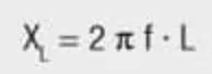
RF inductors behave differently from ideal inductors due to parasitic resistance and capacitance that become significant at high frequencies. The inductive reactance still follows
XL.= 2πfL
,but the effective impedance is shaped by losses and self‑resonant behavior in the intended operating band.
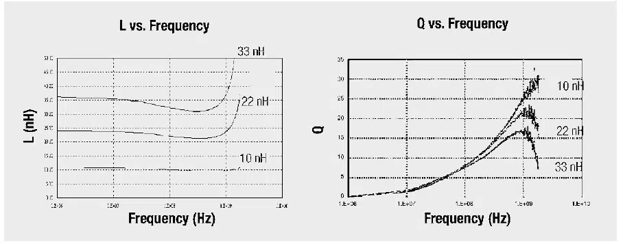
Frequency‑dependent behavior and SRF
Practical RF inductors always exhibit some parasitic capacitance between turns and to their terminals. Together with the inductance this defines a self‑resonant frequency (SRF); below SRF the component is predominantly inductive, while above SRF it behaves capacitively. In most RF designs, the inductor is operated with sufficient margin below its SRF to maintain predictable impedance and avoid unwanted resonances.
Quality factor Q and losses
The quality factor Q of an RF inductor is a measure of how low its losses are at a given frequency. High‑Q inductors are preferred for narrow‑band filters, resonant tanks and oscillators, while broadband matching and EMI suppression may accept lower Q but require stable impedance over a wider range. Q is limited by conductor loss, core loss (if present) and all parasitic effects in the structure.
Core and construction aspects
At RF, many catalog inductors use air, ceramic or low‑loss core materials to push SRF and Q as high as possible. Air‑core and ceramic‑core designs are common for VHF/UHF matching and resonance, whereas ferrite‑based RF chokes are more suitable at lower RF frequencies and for biasing or EMI suppression where higher losses are actually helpful.
The most important electrical properties for selecting RF inductors are:
- Inductance value: Determines the opposition to changes in current and sets the basic reactance at the operating frequency.
- Self‑resonant frequency (SRF): The frequency at which parasitic capacitance cancels the inductance and defines the maximum effective operating frequency.
- Q‑factor: A measure of efficiency; higher Q indicates lower energy losses and is especially important in filters and tuned circuits.
- DC resistance (DCR): Lower DCR reduces resistive loss and improves efficiency, which is critical in many high‑frequency circuits.
How Are RF Inductors Different from Power Inductors?
RF inductors are passive components specifically optimised for operation in the megahertz to gigahertz range, where parasitic effects dominate behaviour. Unlike power inductors, which are designed primarily for energy storage and filtering in switch‑mode power supplies and other low‑to‑medium frequency power applications, RF inductors prioritise low loss, high self‑resonant frequency and controlled impedance in a defined RF band.
The key differences can be summarised as follows:
- Frequency range: RF inductors are intended for RF and microwave frequencies, whereas power inductors typically operate at much lower frequencies.
- Core material: RF inductors often use air or low‑loss ceramic cores to minimise losses and to maintain stability at high frequencies, while power inductors use ferrite cores to reach higher inductance and current capability.
- Current handling: Power inductors are optimised to handle significant DC and AC currents, whereas RF inductors are optimised to maintain signal integrity with minimal distortion and loss at relatively lower currents.
RF Inductor Technology Comparison
Selecting the appropriate inductor technology requires understanding the trade-offs between performance, size, cost, and manufacturing complexity.
| Technology | Material/Structure | Key Attributes | Challenges | Typical Applications |
|---|---|---|---|---|
| Wire-Wound | Copper wire on ceramic/ferrite core | High Q-factor (30-100), high current capability, excellent linearity | Larger size, lower SRF, susceptible to magnetic coupling | Power amplifiers, bias chokes, high-current applications |
| Multilayer Ceramic | Ceramic layers with embedded conductors | Compact size (0402-1210), moderate Q (20-50), good temperature stability | Lower Q than wire-wound, limited current, tighter tolerances needed | Portable devices, smartphones, IoT modules, matching networks |
| Thin-Film | Patterned metal on substrate | Very high Q (50-200), excellent repeatability, tight tolerances | Higher cost, limited inductance range (typically <100 nH) | Precision RF circuits, high-frequency filters, VCOs |
| Air-Core | Self-supporting coil or spring structure | Highest Q possible, no core saturation, excellent linearity | Very large size, susceptible to EMI, difficult to shield | Laboratory equipment, high-power RF, where size is not constrained |
Plating Material Considerations: Gold plating offers superior conductivity, corrosion resistance, and lower loss at high frequencies compared to tin plating. For Q-critical circuits (VCOs, low-noise amplifiers, precision filters), gold plating can provide 10-30% improvement in Q-factor at frequencies above 5 GHz. Tin plating is more cost-effective but may exhibit higher ESR and potential whisker growth in certain environments.
Critical RF Inductor Parameters
Self-Resonant Frequency (SRF): The frequency at which parasitic capacitance resonates with inductance, causing impedance to peak and phase to transition from inductive to capacitive. Golden Rule: SRF should be ≥10× operating frequency to ensure inductive behavior and predictable impedance. Operating too close to SRF causes unpredictable impedance phase, reduced Q-factor, and potential circuit instability.
Inductance Tolerance: Nominal inductance (typically 1 nH to 1 μH for RF applications) with tolerances ranging from ±0.1 nH (tight) to ±20% (standard). Tighter tolerances reduce the need for tuning but increase cost. Include 10-20% margin for PCB parasitics and temperature variation.
Saturation and Rated Current: Saturation current (Isat) is the level at which inductance drops by a specified percentage (typically 10-30%) due to core saturation. Rated current (Irms) is the maximum RMS current based on thermal considerations and self-heating limits.
Advanced Design Considerations
Parasitic Capacitance Management: Minimizing inter-turn and inter-layer capacitance is essential for achieving high SRF. Techniques include optimized winding patterns, increased turn spacing, and progressive winding (varying turn diameter).
Mutual Coupling and Polarity: When inductors are placed close together, magnetic coupling can significantly alter effective inductance and circuit behavior. Polarity markings (dots) indicate winding direction, critical for coupled inductor designs, transformers, and differential circuits. Proper orientation can either enhance or cancel coupling effects.
Core Material Selection:
- Air cores: Highest Q, no saturation, but largest size
- Ceramic cores: Good stability, moderate Q, temperature-stable
- Ferrite cores: High inductance density, but frequency-limited and temperature-sensitive
Real-World Application Examples
Modern RF inductor applications span diverse frequency bands and performance requirements:
- 5G/6G Infrastructure: Matching networks for massive MIMO arrays operating at 3.5 GHz, 28 GHz, and 39 GHz
- Wi-Fi 6E/7: Filters and matching for 6 GHz band with >160 MHz channel bandwidth
- Automotive Radar: 77 GHz and 79 GHz FMCW radar systems requiring ultra-low loss inductors
- Medical MRI: High-Q resonators for precise frequency tuning in gradient coils
Industry Trends and Modern Design Challenges
Miniaturization and High-Frequency Support: Consumer electronics demand ever-smaller components (0201 and smaller) while emerging applications at 6 GHz and beyond (Wi-Fi 6E, 5G mmWave) require inductors with SRF exceeding 60 GHz.
Advanced Design Tools: Modern EM simulators (HFSS, CST, Momentum) provide S-parameter models, but accuracy depends on precise material characterization. Validated vendor models are essential for reliable predictions.
Tolerance and Tuning: Meeting ±0.1 nH tolerances at production scale requires advanced manufacturing control and inline testing, driving up costs but eliminating manual tuning. Many designs include tuning margin to compensate for component tolerances and PCB parasitics.
Air Coil KI; RFH; RFI
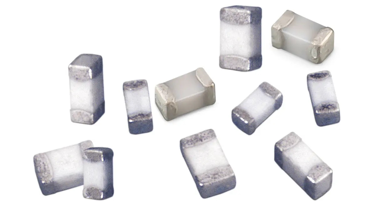
The classic inductor is a configuration of one or more wire windings on a magnetically non-conducting coil former. In contrast to coils with magnetic coil formers or cores, this component‘s advantage is in its current independent inductance and the fact that it shows no saturation effect. Further very important advantages are the linear impedance over a wide frequency range, eq. [4] and a very high quality factor Q (typ. 50–100). The relationship for an inductance L and the winding turns n can be then approximated as shown in eq. [5].

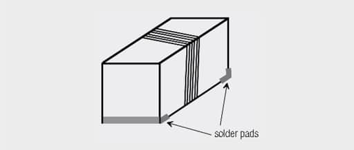
The air coil has a parasitic capacitance dependent on winding diameter, wire thickness as well as layer and winding structure, which mainly exists between neighboring windings (Figure 22.), but for SMD components also occurs between both the connection pads.
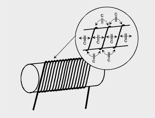
The self-resonant frequency, above which the component shows capacitive characteristics, results from the inductance and the parasitic capacitance.
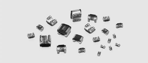
The series of KI ceramic SMD inductors are examples of air coils (Figure 23.).
The solder pads on the coil former are designed to be very small (Figure 24.), in order that the inductors achieve a high self-resonant frequency. Self-resonant frequencies of well above 10 GHz are thus attained.
If higher current carrying capacities are required, the components can be wound on ceramic or ferrite cores depending on the inductance value.
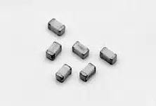
RF Multilayer Ceramic Inductor
The construction of an SMD inductor (Figure 25.) differs from that of a conventional air coil in that the “coil” is printed on a ceramic substrate. This presents the following advantages:
- Very low inductances achievable
- Very low parasitic capacitance and therefore high resonant frequency
- Relatively high current carrying capacity of typ. 300 mA
The specifications of 0201 multilayer ceramic SMD inductor is shown in Figure 26.
The preferred field of application of these components lies in the high-frequency range, in filter circuits and oscillator circuits.
Other RF Inductor Technologies
Besides air coils and multilayer ceramic inductors, RF designers commonly use several other inductor families. Thin‑film RF inductors in very small packages (down to 01005) target high‑frequency matching and integration in dense RF front‑ends where very low inductance values and tight tolerances are required. Ferrite‑core RF chokes provide higher inductance in a compact size and are mainly used as RF chokes on bias lines or for EMI suppression where increased loss is acceptable or desired.
The choice of technology and package size is closely linked to the application. Compact multilayer or thin‑film inductors in 0201/01005 are typically used in mobile and IoT RF front‑ends, while slightly larger air‑core or ceramic‑core coils are attractive in discrete matching networks and resonant circuits in modules. Ferrite‑based RF chokes are widely used on supply lines, reference lines and interfaces where RF isolation is required in addition to DC conduction.
RF Inductor Applications Overview
RF inductors appear in a wide variety of high‑frequency circuits wherever impedance, phase and bandwidth must be controlled accurately. Typical application areas include RF filters and oscillators, impedance‑matching and bias networks, low‑noise amplifiers, medical imaging and RF test equipment.
- RF filters and oscillators: RF inductors, in combination with capacitors, form resonant tanks and selective filters that define or restrict frequency bands in receivers, transmitters and local oscillators.
- Impedance matching and biasing: In matching networks and amplifier bias circuits, RF inductors provide reactive impedance and RF chokes to route DC while isolating and shaping RF signals.
- Low‑noise and medical applications: In MRI preamplifiers and other low‑noise RF front‑ends, carefully chosen RF inductors with high Q and low DCR help maintain signal integrity and minimise noise.
- Radar, communication and test systems: RF inductors support impedance control, filtering and resonance in radar front‑ends, wireless infrastructure and RF measurement equipment across bands such as VHF, UHF and S‑band.
The following table is not a strict design rule set but illustrates how the emphasis shifts from SRF and Q in RF circuits towards DCR and current capability in power‑focused applications.
| Application focus | Inductance level | SRF requirement | Q‑factor target | DCR requirement |
|---|---|---|---|---|
| High‑frequency resonance and RF filters | Low to medium | Very high | Very high | Low |
| Power‑side coupling / energy transfer | Medium to high | High | Low to medium | Very low |
| Power filter chokes | High | Medium to high | Low | Very low |
| SMPS / DC‑DC power inductors | Medium to high | Medium | Low | Very low |
Selecting RF Inductors for Filters and Matching
When selecting RF inductors for filters, matching networks or chokes, both electrical parameters and practical implementation details must be considered. Catalog data at the relevant frequency is more important than nominal inductance at 100 kHz or 1 MHz.
Electrical selection
- Choose the nominal inductance and tolerance to match the intended filter or matching topology, then verify the impedance value at the operating frequency in the datasheet curves.
- Ensure that the inductor’s self‑resonant frequency is significantly higher than the highest operating frequency, typically by at least a factor of two, to maintain a predominantly inductive behavior.
- Select an appropriate Q level: high Q for narrow‑band filters, resonant circuits and VCOs, moderate Q and stable impedance for broadband matching or EMI suppression.
Current, power and bias
- Check the specified DC and RF current ratings and consider temperature rise limits in the application.
- For inductors with magnetic cores, DC bias can reduce inductance and Q; datasheets often provide L vs. DC bias curves that should be consulted at the intended operating point.
Layout and EMC considerations
- Minimise loop area and via inductance in the PCB layout to preserve the intended impedance and reduce stray coupling.
- Place RF inductors away from strong magnetic fields from power inductors or transformers, and avoid routing noisy digital or power traces directly underneath sensitive RF inductors.
- For high‑frequency SMD inductors, follow the manufacturer’s recommended land patterns and layout notes to achieve the published performance.
Tolerance, spread and tuning
- Typical RF inductors follow E‑series values with tolerances in the ±2% to ±10% range, depending on technology.
- In many RF designs some tuning margin is foreseen, for example through provision for alternative inductor values or small layout changes, to compensate for component tolerances and PCB parasitics.
8-Step RF Inductor Selection Process
For systematic component selection in critical RF designs, follow this methodology:
Step 1: Define Operating Frequency and Bandwidth
Identify the center frequency and required bandwidth. Calculate minimum acceptable SRF using the rule: SRF ≥ 10 × f_operating. For example, a 2.4 GHz application requires SRF ≥ 24 GHz.
Step 2: Determine Required Inductance Value
Use circuit simulation or analytical formulas to calculate target inductance. For impedance matching, use Smith chart transformations or matching network calculators. For LC resonators, apply f₀ = 1/(2π√LC).
Step 3: Specify Tolerance and Tuning Margin
Decide whether to use standard tolerances (±5-10%) with tuning capability or tight tolerances (±0.1 nH, ±2%) without tuning. Allocate 10-20% margin beyond calculated tolerance to account for PCB parasitics, component aging, and temperature variation.
Step 4: Calculate Current Requirements
Determine both DC and RF current levels. DC bias current must be below Isat rating to prevent core saturation. RMS current must be below Irms rating to prevent thermal damage.
Step 5: Evaluate Q-Factor Requirements
Target Q values based on application: General purpose Q > 20, low-loss matching Q > 40, high-selectivity filters Q > 60, VCO/oscillators Q > 80.
Step 6: Select Technology and Package Size
Choose technology based on priorities: Maximum Q (thin-film or air-core), minimum size (multilayer ceramic 0402/0201), high current (wire-wound), or cost-sensitive (standard multilayer with relaxed tolerances).
Step 7: Verify with Simulation and S-Parameters
Import vendor-provided S-parameter models into circuit simulator (ADS, Genesys, Microwave Office). Verify impedance magnitude and phase, return loss (S11), insertion loss (S21), and group delay across operating bandwidth.
Step 8: Prototype Validation with VNA
After PCB fabrication, use a Vector Network Analyzer (VNA) to measure actual performance:
- VNA Calibration: Perform full 2-port SOLT (Short-Open-Load-Thru) calibration to the reference planes. Poor calibration is the #1 source of measurement errors.
- Diagnostic Techniques: Measure S11 (input impedance) to verify matching network transformation. Measure S21 (insertion loss) to quantify filter performance. Smith chart display shows impedance locus vs. frequency. Use TDR mode to identify discontinuities and parasitics.
- Common Issues: Impedance mismatch (adjust component values or add tuning elements), lower-than-expected Q (check solder joints, via inductance, ground plane continuity), SRF shift (verify PCB parasitics), bandwidth too narrow/wide (adjust component Q or coupling).
Reliability, Testing and Standards
EMI filters and RF inductors are often used in applications with demanding environmental and reliability requirements. Relevant qualification standards include, for example, AEC‑Q200 for many SMD inductors and EMI filters in automotive electronics, and MIL‑STD‑220 for insertion loss definitions and test methods.
Typical failure modes in EMI and RF filters include short circuits due to cracks in ceramic elements with subsequent metal migration, and open circuits caused by mechanical damage or poor internal solder joints. RF inductors can fail open due to wire breaks or solder joint cracks, or show degraded Q and shifted inductance as a result of mechanical stress, contamination or thermal aging.
From a design‑in perspective it is important to respect the specified operating temperature range, DC and RF current ratings and derating recommendations. Operating components with margin below maximum voltage, current and temperature, and with sufficient distance to SRF, improves long‑term stability and reduces the risk of unexpected behavior in critical RF and EMI functions.
Visual Learning Resource: RF Inductor Selection
For additional insight into RF inductor selection and application, this technical presentation from Würth Elektronik covers practical design considerations:
The presentation explores impedance matching fundamentals, measurement techniques, and real-world examples of RF inductor implementation in wireless circuits.
Summary
This article has reviewed the fundamentals of passive filters and RF inductors, starting from basic LC/RC concepts, attenuation and insertion loss through to practical EMI/RFI filter structures and power line filters. It has outlined how LTCC technology integrates inductors, capacitors and other RF structures into compact, highly reproducible RF filters, baluns and chip antennas for modern wireless systems.
In the RF inductor section, different inductor technologies such as air‑core, multilayer ceramic, thin‑film and ferrite‑core chokes have been compared together with their typical frequency ranges and applications. Key RF‑specific parameters including SRF, Q‑factor, DCR and current handling were introduced, followed by selection guidelines, layout recommendations and an overview of reliability aspects and standards relevant for demanding automotive and industrial applications.
Conclusion
RF inductors play a central role in shaping the behaviour of RF filters, matching networks and front‑end circuits, and their performance is strongly influenced by construction technology, core material and parasitic elements. Understanding the trade‑offs between SRF, Q, DCR, current capability and reliability enables engineers to choose the most suitable component family for each application, from compact LTCC‑based filters to discrete air‑core coils and ferrite‑core RF chokes.
Combined with careful PCB layout and appropriate derating, the right choice of RF inductors and filter structures helps to ensure robust EMC performance, efficient spectrum use and long‑term stability in communication, medical, industrial and automotive systems. The concepts presented here are intended as a practical reference for both initial architecture decisions and detailed RF design‑in work.
FAQ – RF Inductors and Filters
RF inductors, together with capacitors, form resonant and low‑pass structures that define frequency response, provide attenuation of unwanted RF signals and help ensure EMC compliance in RF and power electronic systems.
RF inductors are optimised for megahertz to gigahertz operation, prioritising high self‑resonant frequency, high Q‑factor and controlled impedance, while power inductors focus on energy storage and high current handling at much lower frequencies.
SRF marks the point where parasitic capacitance cancels the inductance and the component becomes capacitive; RF inductors must be operated with sufficient margin below SRF to maintain predictable inductive behaviour and stable filter performance.
Typical technologies include air‑core and ceramic‑core wire‑wound coils, multilayer ceramic inductors, thin‑film inductors for very small values and ferrite‑core RF chokes used mainly for biasing and EMI suppression.
The key parameters are inductance value, self‑resonant frequency, Q‑factor, DC resistance and current rating, all evaluated at the actual operating frequency rather than only at catalogue test frequencies.
LTCC technology integrates inductors, capacitors, baluns and sometimes antennas into compact multilayer structures with low parasitics, enabling reproducible, space‑saving RF filters and front‑end modules for modern wireless systems.
Good practice includes minimising loop area and via inductance, keeping RF inductors away from power magnetics and noisy traces, following manufacturer land‑pattern guidelines and maintaining a solid RF ground reference.
Many SMD inductors and EMI filters follow AEC‑Q200 qualification for automotive use, while insertion loss definitions and test methods often reference MIL‑STD‑220 in RF and EMI filter characterisation.
Polarity markings indicate the winding direction and phase relationship between inductor terminals, essential for circuits using coupled inductors, transformers, differential pairs, or balanced networks. When two inductors are magnetically coupled, their relative polarity determines whether coupling is additive (aiding) or subtractive (opposing). Incorrect polarity can cause transformer malfunction, differential mode conversion to common mode, or unexpected resonance frequencies in coupled resonators.
Start with proper 2-port SOLT calibration to your reference planes. Measure S11 (reflection coefficient) and display on a Smith chart—the impedance locus should transform from source impedance to load impedance across your frequency band. If matching is poor: (1) verify component values against design, (2) check for PCB layout parasitics (via inductance, trace width variations), (3) measure component impedances individually to confirm specifications, (4) use TDR mode to locate discontinuities, and (5) adjust component values iteratively while measuring.
Gold plating offers superior electrical conductivity, better corrosion resistance, and lower skin effect losses at high frequencies, making it preferred for high-performance RF applications above 2 GHz. Tin plating is more cost-effective and provides adequate performance for moderate-frequency applications (<2 GHz) but exhibits slightly higher ESR and potential tin whisker growth concerns in high-reliability applications. For Q-critical circuits, gold plating can provide 10-30% improvement in Q-factor at frequencies above 5 GHz.
Tolerance selection involves trade-offs between cost, tuning requirements, and yield:
±5% to ±10%: Standard tolerance, lowest cost, requires circuit tuning or wide matching bandwidth
±2% to ±5%: Common for production designs with some tuning margin
±0.1 nH or ±2%: Tight tolerance for tuning-free designs, higher cost but improved production yield
Calculate required tolerance based on bandwidth, acceptable VSWR variation, and available tuning methods. Include 10-20% margin for PCB parasitics and temperature variation.
How to Select an RF Inductor for Filters and Matching Networks
- Step 1: Define the RF application and frequency range
Identify whether the inductor will be used in a low‑pass or band‑pass filter, a resonant tank, an impedance‑matching network or as an RF choke, and determine the operating frequency band for the design.
- Step 2: Determine the required inductance and tolerance
Derive the nominal inductance value and tolerance from your filter or matching equations, then check that catalogue parts offer this value with realistic tolerances and E‑series steps suitable for tuning.
- Step 3: Check self‑resonant frequency (SRF) margin
From the datasheet, verify that the inductor’s self‑resonant frequency is at least about two times higher than the highest operating frequency, so that the inductor behaves predominantly inductively in the application band.
- Step 4: Evaluate Q‑factor at the operating frequency
Review Q‑factor versus frequency curves in the datasheet and ensure that Q is sufficiently high for narrow‑band filters and resonant circuits, or adequately stable for broadband matching and EMI suppression functions.
- Step 5: Verify DC resistance and current ratings
Check DC resistance and current ratings to keep resistive losses, voltage drop and temperature rise within acceptable limits, and for core‑based inductors confirm DC bias effects on inductance at the intended operating current.
- Step 6: Choose the appropriate technology and package
Select between air‑core, multilayer ceramic, thin‑film or ferrite‑core RF chokes based on required inductance, SRF, Q, size constraints and whether the main emphasis is RF performance or power/EMI behaviour.
- Step 7: Plan PCB layout for RF integrity
Place the inductor to minimise loop area and parasitic coupling, keep it away from strong magnetic fields and noisy traces, and follow the manufacturer’s recommended pad layout to achieve the specified RF performance.
- Step 8: Consider reliability, derating and standards
Apply derating for voltage, current and temperature where appropriate, confirm that critical parts meet relevant standards such as AEC‑Q200, and ensure that the design leaves margin to SRF for long‑term stability.
Further Read:
- What Electronics Engineer Needs to Know About Passive Low Pass Filters for a deeper discussion on low‑pass filter theory and design.