


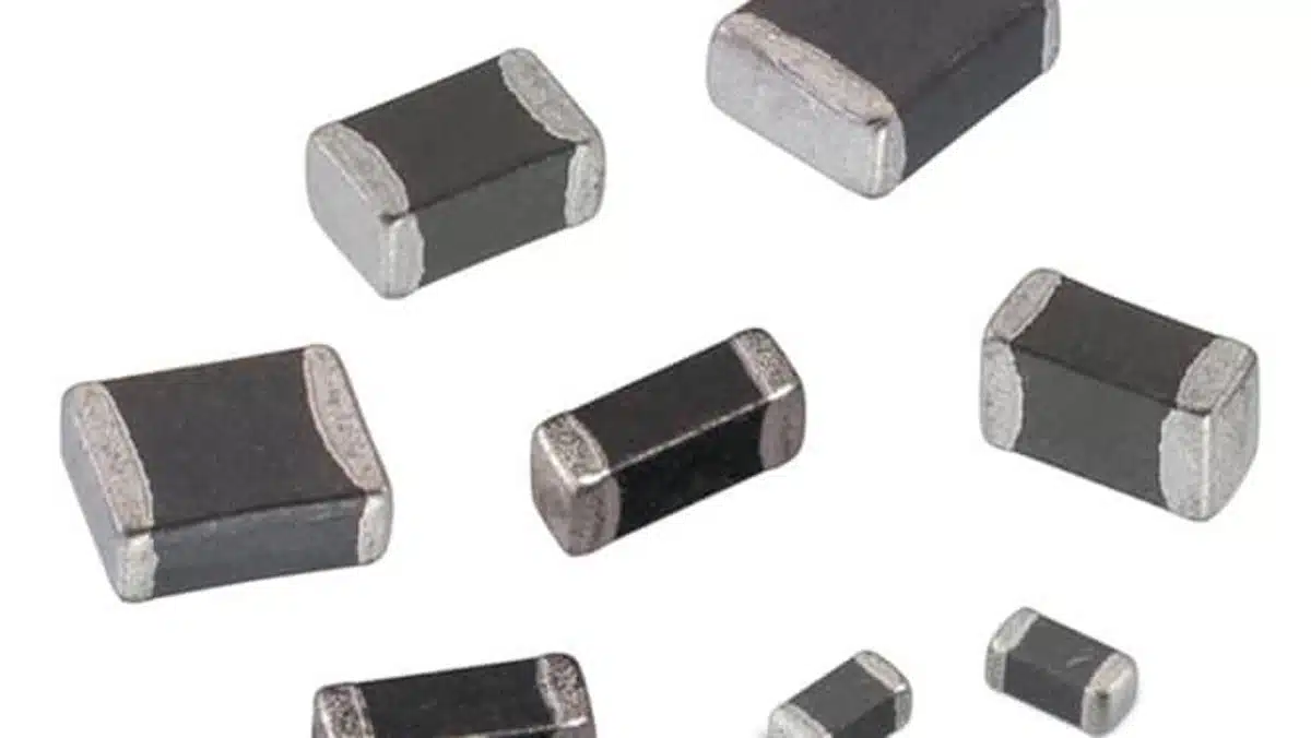
SMD surface mount inductors can be easily placed by high‑speed pick‑and‑place machines and thus reduce assembly cost compared to through‑hole coils.
The SMD technology also supports a high level of miniaturization and downsizing of electronics, which makes SMD inductors the default choice in most modern designs.
Key Takeaways
- SMD inductors reduce assembly costs and support miniaturization, making them essential for modern electronics.
- Multilayer SMD inductors offer excellent shielding and stability, suitable for filters and dense circuits.
- Power multilayer inductors achieve high efficiency at compact sizes, usually used in portable devices.
- Different SMD inductor types exist, each optimized for specific applications, including RF and power management.
- Selection of SMD inductors depends on parameters like inductance, saturation current, and DC resistance.
SMD Multilayer inductors
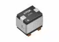
If the wire windings on the outside of a conventional “coil” are mounted inside the coil body, the so-called multilayer SMD inductor (Figure 1. and 2.) is created.
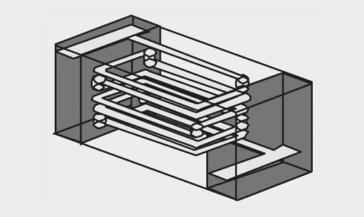
The ferrite body magnetically shields the component, significantly reducing external interference and cross-talk. The multilayer inductor may be seen as a “compromise” between the ceramic inductor and SMD ferrite. This component is especially suitable as an inductor in filters and resonant circuits where low interference from external signals is required and in circuits with high packing density.
In addition, multilayer inductors offer very good repeatability of inductance values and parasitics thanks to the printed, photolithographic manufacturing process, which simplifies filter and impedance matching design compared to hand‑wound constructions.
passive-components
Practical tips:
- Do not operate close to the self‑resonant frequency range, because the component’s behaviour changes from inductive to capacitive and Q collapses.
- Observe max. current loading capacity
- Low DC resistance, therefore also suitable for low-voltage systems
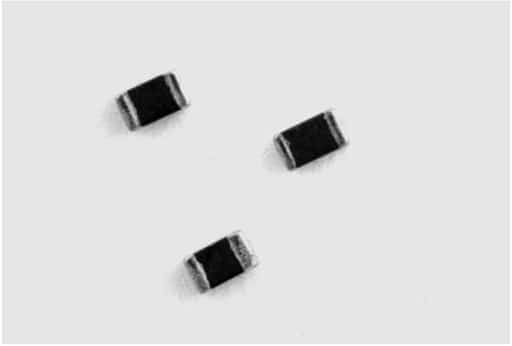
Power Multilayer Inductors
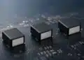
The miniaturization of SMD components, especially inductors, is a widespread trend in portable devices, as it is especially storage chokes that frequently require the most space. Wired components are out of the question in these orders of magnitude. This is where the power multilayer types (Figure 3.) apply.
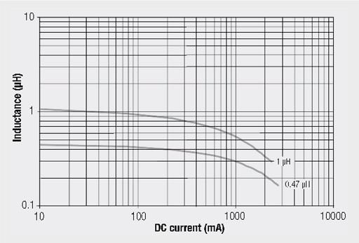
In order to allow minimization of the coil volume, the switching controller IC is driven at ever-higher switching frequencies. Switching controllers like the Micrel MIC2285 already work with 4 MHz. The dimensions of the storage chokes required can therefore be reduced by up to 90%. The compact power multilayer inductors in 1008 package (2.5 mm x 2.0 mm x 1.0 mm) not only offer high rated currents (up to 2.4 A), but also a lower DCR than comparable to standard multilayer inductors types.
Compared to discrete wire‑wound chokes with similar current capability, these multilayer parts trade some efficiency for a much smaller, fully shielded form factor that is better suited to densely packed handheld and wearables PCBs.
The saturation current of the power multilayer inductors (such as WE-PMIs) relates to the typical inductance drop of –30% from the zero current inductance. The rated current is defined for the common self-heating of DT = 40 K with respect to the ambient temperature.

The used NiZn core material allows the use of the power inductors WE‑PMI series up to 10 MHz. In practice, most designers operate such inductors well below this limit, typically in the 1–4 MHz range, in order to balance core losses, switching losses in the converter and achievable efficiency.
.
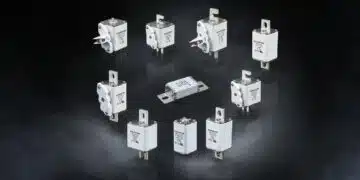
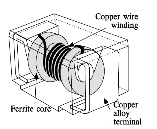
SMD – Wire Wound Inductor /SMD RF Inductor
Wound inductors are available also in SMD packages (Figure 6.). Individual types may essentially differ in their mechanical construction. Whereas components as WE-GF in Figure 6. right is completely embedded in plastic and can therefore handle high humidity very effectively, the other types (WE-LQ – Figure 6. left) is in an open package.
It can therefore be loaded with higher currents at the same inductance in relation to its package volume. However, the open construction also exposes the winding and core to the environment, so moisture, contamination and mechanical handling must be considered, especially in high‑reliability or automotive designs.
In Figure 7. and 8. the layout of the SMD RF Inductor is shown graphically. A wire-wrapping surrounds a ferrite body. The special ferrite mixture faciliates a wide inductance spectrum despite the miniature ferrite core. For RF matching applications, these inductors are usually specified by their impedance and Q over frequency rather than purely by inductance at 100 kHz, so it is important to read the RF datasheet curves instead of only the nominal L value.

Selection and Application Guidelines
Modern SMD inductors span several construction types and core materials, each optimized for a specific frequency range and application domain. This section provides practical guidelines for selecting the right inductor for power, signal and RF designs, complementing the basic construction overview above and helping to bridge from catalogue choice to real‑world design‑in.
Overview of SMD Inductor Types
The table below summarizes the main SMD chip inductor families you typically encounter on the market.
The goal is not to list every product series, but to highlight how construction, shielding and package style map to typical use cases and design trade‑offs.
| Inductor type | Typical construction / example | Frequency range | Typical use cases | Key advantages | Typical limitations |
|---|---|---|---|---|---|
| Multilayer signal | Screen‑printed ferrite, stacked ceramic body | kHz to low MHz | Filters, resonant circuits, bias chokes | Good shielding, small sizes, low cost | Limited current, lower Q, lower SRF |
| Power multilayer | Internal printed windings in ferrite body | 100 kHz to ~10 MHz | DC/DC converters in portable devices | Very small footprint, shielded, low DCR | Lower Isat than comparable wire‑wound |
| Wire‑wound open (power) | Enamelled wire on ferrite core, open frame | 100 kHz to a few MHz | General power chokes, point‑of‑load | High current, higher Q, low DCR | More EMI, less moisture protection |
| Wire‑wound molded / sealed | Wire on core fully molded/encapsulated | 1 MHz to RF | RF chokes, matching, high‑rel designs | Good environmental robustness, shielding | Slightly higher DCR, larger package |
| Thin‑film / air‑core RF | Planar or wire‑wound on low‑loss cores | Tens of MHz to GHz | RF matching, impedance networks | Very high SRF and Q | Very low inductance, small currents |
Core Materials and Frequency Range
Core material selection defines usable frequency band, losses and DC bias behaviour.
- Ferrite NiZn: Used in many multilayer and small power SMD inductors; suitable up to about 10 MHz for power applications and higher for small‑signal RF chokes.
- Ferrite MnZn: Higher permeability, used at lower frequencies, but with higher core losses at several MHz.
- Powdered iron / alloy / metal powder: Distributed air gap, good for power chokes with higher saturation current and better DC bias behaviour in the hundreds of kHz to low MHz range.
- Nanocrystalline / amorphous cores: Enable low‑loss operation in the MHz region for advanced chip inductors; see the dedicated article on nanocrystalline MHz cores.
In many real designs, the choice of core material is implicit in the inductor series you pick from a manufacturer catalogue. Understanding the underlying material behaviour, however, helps you to explain why some “equivalent” inductors run hotter or saturate earlier than others, even when their nominal L and current ratings look similar on paper.
| Core material | Relative permeability | Losses at MHz | Saturation flux / DC bias | Typical application band |
|---|---|---|---|---|
| NiZn ferrite | Medium | Moderate at 1–10 MHz | Moderate | Power multilayer, small RF chokes |
| MnZn ferrite | High | Higher above ~1 MHz | Moderate‑high | Low‑frequency chokes, filters |
| Powdered iron / alloy | Low‑medium | Lower at power freq | High | Power chokes 100 kHz–1 MHz |
| Nanocrystalline | Medium‑high | Very low up to MHz | High | Low‑loss MHz chip inductors |
Key Electrical Parameters for Selection
When selecting an SMD chip inductor, the following parameters are usually critical:
- Inductance (L): Sets impedance and determines filter corner frequency or energy storage.
- Saturation current (Isat): Current where inductance drops (often by 20–30%) due to core saturation; for many power multilayer series this is specified at about −30% from zero‑current inductance.
- Rated current (Irated): Current that causes a specified temperature rise (for example 40 K) above ambient.
- DC resistance (DCR): Drives conduction losses; especially important in low‑voltage supplies.
- Self‑resonant frequency (SRF): Above SRF the part becomes capacitive and should not be used as an inductor.
- Quality factor (Q): Relevant for resonant circuits and RF matching; higher Q means lower losses around the operating frequency.
For compact power supplies it is often necessary to iterate between these parameters: reducing DCR by going to a larger package or different series may increase SRF and current ratings, but also cost and footprint, while a high‑Q RF inductor might not tolerate the required DC bias current in a bias‑tee or choke role.
Table 3 indicates which parameters typically dominate for different application classes.
| Application | L range | Priority parameters | Preferred types |
|---|---|---|---|
| Buck/boost DC/DC choke | 0.22–10 µH | Isat, Irated, DCR, thermal behaviour | Power multilayer, wire‑wound power |
| Input/output EMI filter | 1–100 µH | L, DCR, SRF, shielding | Multilayer, shielded wire‑wound |
| RF matching (VHF/UHF) | 3–270 nH | SRF, Q, tolerance, temperature stability | Wire‑wound RF, thin‑film |
| Resonant LC filters (audio/IF) | 1 µH–10 mH | L accuracy, Q, DCR | Wire‑wound, multilayer |
| Bias chokes / decoupling | 10 nH–10 µH | SRF, impedance vs frequency, DC current | Multilayer ferrite, RF chokes |
Practical Design‑In Guidelines
- Avoid operation near SRF
Always check the datasheet impedance versus frequency and locate SRF for the chosen inductance value.
Keep your operating band at least one octave below SRF for power and filter applications, unless you deliberately use the resonance peak in RF filters. - Check current ratings with margin
For power chokes, calculate peak inductor current and ensure it stays comfortably below Isat with a safety margin of typically 20–30%. Ensure RMS current remains below Irated so that temperature rise stays within your thermal budget, and remember that available copper area and PCB stack‑up can significantly influence the real‑world temperature of small SMD chokes.
- Minimize conduction and core losses
Select the lowest feasible DCR within your size and cost constraints, especially in low‑voltage converters where even tens of milliohms matter.
For switching converters above 1–2 MHz, prefer low‑loss cores explicitly specified for that frequency band, and verify efficiency with bench measurements, as small differences in core loss can become dominant at high frequency and low output power. - Pay attention to shielding and layout
In dense layouts, shielded multilayer or molded wire‑wound inductors reduce radiated fields and cross‑talk to neighbouring traces and components.
Place high‑di/dt power inductors close to the switching device and use wide, short copper traces or polygons to lower parasitics and improve thermal spreading. - Consider environment and reliability
Open wire‑wound types can handle higher currents in the same volume but may be more sensitive to humidity and contamination than fully encapsulated RF inductors.
For automotive or aerospace, select AEC‑Q200 qualified series and review derating curves for temperature and current, and where possible combine this with endurance or wear‑out data from application notes or dedicated studies.
Quick Selection Example
For a 5 V to 3.3 V buck converter at 2 MHz and 1 A load, you would first choose a target ripple current (for example 30–40% of the output current) and compute the required inductance, which often falls around 1–2 µH.
Then search for power multilayer or small wire‑wound SMD inductors in 1008 or 1210 case sizes with approximately 1.5 µH, sufficient Isat and Irated (≥ 1.5 A and ≥ 1 A respectively), low DCR and an SRF several times higher than the 2 MHz switching frequency.
Finally, compare NiZn‑based multilayer options against metal‑powder wire‑wound chokes: multilayer parts minimize footprint and EMI, while wire‑wound types often offer higher efficiency at higher currents.
As a final sanity check, simulate the converter with realistic DCR and core‑loss estimates and then verify with bench measurements of ripple current, efficiency and temperature rise, adjusting the inductor choice if necessary.
Conclusion
The basic construction overview of multilayer and wire‑wound SMD inductors explains why different technologies exist, but successful design‑in requires a structured selection approach.
By classifying the inductor type, choosing an appropriate core material and frequency range, and then checking inductance, current ratings, DCR, SRF and Q against the target application, designers can converge quickly on suitable SMD chip inductors.
Power multilayer inductors are attractive where footprint and height are critical, while wire‑wound and advanced core technologies such as metal powder and nanocrystalline cores are preferred for the highest efficiency, current capability and MHz‑range performance.
Combined with the detailed articles on nanocrystalline cores, wear‑out mechanisms and nonlinear inductor characterization available on this blog, this overview gives designers a coherent, end‑to‑end picture of how to specify, select and validate SMD chip inductors for demanding applications.
FAQ
SMD chip inductors are miniature inductors in surface‑mount packages that can be placed by high‑speed pick‑and‑place machines instead of manual insertion of through‑hole coils. They reduce assembly cost and enable high packing density and miniaturization in modern electronic devices.
Multilayer SMD inductors use printed windings in a ceramic/ferrite body and offer very small, well‑shielded components ideal for signal and small power applications. Wire‑wound SMD inductors use an enamelled wire wound on a core and can handle higher currents and achieve higher Q, at the cost of larger size or less shielding.
For power supplies the key parameters are inductance value, saturation current, rated current, DC resistance (DCR) and self‑resonant frequency (SRF). Designers typically choose an inductance that gives acceptable ripple, then check Isat, Irated and DCR to meet efficiency and temperature‑rise targets while keeping operation safely below SRF
SRF is the frequency at which the inductor’s parasitic capacitance resonates with its inductance and its behaviour changes from inductive to capacitive. Operating close to SRF leads to high losses and unpredictable impedance, so most designs keep the working frequency at least one octave below SRF.
Core materials such as NiZn ferrite, MnZn ferrite, powdered iron, alloy and nanocrystalline each have distinct permeability, loss and saturation characteristics. They define the usable frequency range, losses and DC bias behaviour, so choosing the right material is crucial for low‑loss operation and stable inductance under load.
Shielded SMD inductors are preferred in dense layouts and high‑frequency designs where stray magnetic fields can couple into nearby traces or components. Multilayer and molded shielded inductors help reduce EMI and make it easier to pass EMC tests compared to open wire‑wound types.
In practice, power and RF applications usually require different inductor series optimized for very different current, Q and frequency ranges. Power chokes are designed for high current and low DCR at hundreds of kHz to a few MHz, while RF inductors prioritize high Q and SRF at tens or hundreds of MHz but only carry small currents.
A practical workflow is to define the application and frequency range, choose a suitable inductor family and core material, then select inductance, Isat, Irated, DCR and SRF with adequate design margin. Finally, simulate and verify the choice on the bench by measuring ripple current, efficiency and temperature rise, adjusting the inductor type or value if needed.
Reference and Further Reading
- SMD Inductors – Passive Components Blog
- Nanocrystalline Cores for Low‑Loss MHz Chip Inductors – Passive Components Blog
- Experimental Evaluation of Wear Failures in SMD Inductors – Passive Components Blog
- One‑Pulse Characterization of Nonlinear Power Inductors – Passive Components Blog
- Würth Elektronik – SMD Inductors (WE‑MI, WE‑PMI, WE‑LQ, WE‑GF and related families)