Mention an electronic circuit and you are likely to picture a printed circuit board (PCB): a rigid rectangle in a characteristic green color with copper lines and a bewildering array of components soldered onto it. But does adding electronic functionality means using a PCB and thus requires shoehorning a rigid rectangle into the product?
The emerging approach of 3D electronics suggests not. Instead of making them separately on a rigid board, 3D electronics instead involves integrating electronic functionality within or onto the surface of objects. While antennas and simple conductive interconnects have long been added to the surface of injection-molded plastic objects, 3D electronics is undergoing extensive innovation with new materials, metallization methods and manufacturing methodologies. This rapidly developing field is extensively analyzed in the new IDTechEx report, “3D Electronics 2020-2030: Technologies, Forecasts, Players”.
Alternative Approaches
Electrical circuits are increasingly being added onto 3D surfaces and integrated within objects using a range of new techniques. While aerosol and material jetting enable conductive interconnects to be applied to surfaces, in-mold electronics and 3D printed electronics enable complete circuits to be integrated within an object. Between them the various approaches offer multiple benefits that include simplified manufacturing, reduced weight and novel form factors. With 3D electronics, adding electronic functionality no longer requires incorporating a rigid, planar PCB into an object then wiring up the relevant switches, sensors, power sources and other external components.
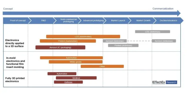
The new report from IDTechEx, “3D Electronics 2020-2030: Technologies, Forecasts, Players”, provides an extensive overview of all approaches to 3D electronics informed by interviews with major players across the space. The pros and cons of each approach are weighed against each other for different applications, with numerous case studies showing how the different manufacturing techniques are deployed across the automotive, consumer goods and medical device sectors. Furthermore, through detailed analysis of the technologies and their requirements, we identify innovation opportunities for both materials and manufacturing methods. All the approaches and technologies analyzed in this report are shown below on a roadmap that shows their progress from concept to commercialization for different applications.
Electronics on a Surface
The best-established approach to adding electrical functionality onto the surface of 3D objects is laser direct structuring (LDS), in which an additive in the injection-molded plastic is selectively activated by a laser. This forms a pattern that is subsequently metallized using electroless plating. LDS saw tremendous growth around a decade ago and is used to manufacture 100s of millions of devices each year, around 75% of which are antennas.
However, despite its high patterning speed and widespread adoption, LDS has some weaknesses that leave space for alternative approaches to surface metallization. Firstly, it is a two-step process that can require sending parts elsewhere for plating, thus risking IP exposure. It has a minimum resolution in mass production of around 75 um, thus limiting the line density, and can only be employed on molded plastic. Most importantly, LDS only enables a single layer of metallization, thus precluding crossovers and hence substantially restricting circuit complexity.
Given these limitations, other approaches to applying conductive traces to the surfaces of 3D objects are gaining ground. Extruding conductive paste, a viscous suspension comprising multiple conductive flakes, is already used for a small proportion of antennas, and is the approach of choice for systems that deposit entire circuits onto 3D surfaces.
Aerosol jetting is another emerging metallization approach, in which a relatively low viscosity, usually conductive ink is atomized. This spray is then combined with an inert carrier gas and ejected from a nozzle. Aerosol jet has two notable advantages: it is capable of resolutions as fine as 10 um, and the nozzle can be placed a few mm away from the surface thus facilitating patterning of 3D surfaces with complex surface geometries. The downsides are the cost of the complex atomization and delivery process, and the requirement to re-optimize the process for different inks.
An advantage of digital deposition methods of the incumbent LDS technology is that dielectric materials can also be deposited within the same printing system, thereby enabling cross-overs and hence much more complex circuits. Insulating and conductive adhesives can also be deposited, enabling SMD components to be mounted onto the surface.
In-mold Electronics
In-mold electronics (IME) offers a commercially compelling proposition of integrating electronics into injection-molded parts, reducing manufacturing complexity, lowering weight and enabling new form factors since rigid PCBs are no longer required. Furthermore, it relies on existing manufacturing techniques such as in-mold decoration and thermoforming, reducing the barriers to adoption. The basic principle is that a circuit is printed onto a thermoformable substrate, and SMD components mounted using conductive adhesives. The substrate is then thermoformed to the desired shape and infilled with injection-molded plastic. IME is especially well suited to human-machine interfaces (HMIs) in both automotive interiors and the control panels of white goods, since decorative films can be used on the outer surface above capacitive touch sensors.
While IME is likely to dominate HMI interfaces in the future due to the ease of manufacture and compatibility with established manufacturing techniques, it does bring technical challenges. Chief among these is developing conductive and dielectric materials that can withstand the temperature of the thermoforming process along with the heat and pressure of injection-molding. As such, materials suppliers are developing portfolios of materials aimed at IME, with conductive inks that can be deformed without cracking. Additional challenges include the development of electronic design software that can account for bending on circuits and developing SMD component attachment methods that are reliable under the molding process.
Fully 3D Printed Electronics
The least developed technology is fully 3D printed electronics, in which dielectric materials (usually thermoplastics) and conductive materials are sequentially deposited. Combined with placed SMD components, this results in a circuit, potentially with a complex multilayer structure embedded in a 3D plastic object. The core value proposition is that each object and embedded circuit can be manufactured to a different design without the expense of manufacturing masks and molds each time.
Fully 3D printed electronics are thus well suited to applications where a wide range of components need to be manufactured at short notice. Indeed, the US Army are currently trialing a ruggedized 3D printer to make replacement components in forward operating bases. The technology is also promising for applications where a customized shape and even functionality is important, for example, medical devices such as hearing aids and prosthetics. The ability of 3D printed electronics to manufacture different components using the same equipment, and the associated decoupling of unit cost and volume, could also enable a transition to on-demand manufacturing, in which objects with electronic functionality are
The challenges for fully 3D printed electronics are that manufacturing is fundamentally a much slower process than making parts via injection-molding since each layer needs to be deposited sequentially. While the printing process can be accelerated using multiple nozzles, it is best targeted at applications where the customizability offers a tangible advantage. Ensuring reliability is also a challenge since with embedded electronics post-hoc repairs are impossible – one strategy is using image analysis to check each layer and perform any repairs before the next layer is deposited.


