


Magnetics in High‑Frequency GaN Converters: Design Lessons for the 0.5–1 MHz Era
This article summarizes key insights from a Frenetic webinar with Sotiris Zorbas and translates them into practical guidance for engineers designing magnetics in high‑frequency GaN applications.
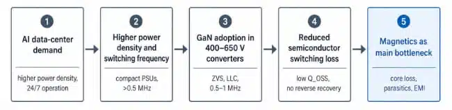
AI data centers and high‑density servers are pushing power converters toward higher power density, higher switching frequencies, and stricter efficiency targets. In this new landscape, GaN devices sit in the sweet spot of 400–650 V converters above , but the limiting factor is no longer the semiconductor—it is the magnetics.
GaN’s sweet spot and its impact on magnetics
GaN has emerged as a strong competitor to silicon carbide in medium‑voltage, high‑frequency applications such as 400 V to 48 V or 12 V stages in data center power supplies. While silicon carbide continues to dominate higher‑voltage, hard‑switched applications (for example on‑board chargers and EV traction inverters), GaN offers unique advantages when operated above .
A key comparison considers three figures of merit: , gate charge, and reverse recovery performance. Modern GaN and silicon carbide devices both achieve roughly one order of magnitude lower output charge than state‑of‑the‑art silicon superjunction MOSFETs, dramatically reducing switching losses. GaN further differentiates itself by eliminating the anti‑parallel body diode, so there is effectively no reverse recovery, which is a major benefit in soft‑switching LLC and other ZVS topologies.
In practice, GaN’s main sweet spot today is:
- DC bus voltages in the 400–650 V range
- Switching frequencies from 0.5 to 1MHz
- Converter topologies with ZVS operation such as LLC resonant stages
In these conditions, overall converter efficiencies around 96–98% (and even up to 99% in some cases) are achievable, but the residual 1–3% of losses concentrate heavily in the magnetics—transformers, inductors, and EMI chokes—making their design critical.
Key features and benefits of GaN‑based converters
Semiconductor advantages relevant to magnetics
When selecting semiconductors for a GaN‑based converter, it is useful to interpret the main device parameters from a magnetics perspective.
Where GaN fits in converter design
| Parameter | Silicon superjunction MOSFET | SiC MOSFET | GaN HEMT |
|---|---|---|---|
| Relative (Q_{\text{OSS}}) trend | Baseline reference | About one order of magnitude lower than silicon MOSFET | About one order of magnitude lower than silicon MOSFET |
| Gate charge trend | Reference | Lower than silicon MOSFET | Low, suited to very high switching frequency |
| Reverse recovery | Present | Low, but not zero | Essentially no reverse recovery contribution from an anti-parallel diode |
| Best-fit operating region | Lower-frequency high-efficiency power conversion | High-voltage, hard-switched converters | 400–650 V converters above about 0.5 MHz |
| Typical examples mentioned in the webinar | General silicon baseline | EV traction and on-board charger classes | LLC and high-density server/data-center power stages |
- Lower QOSS: Both GaN and silicon carbide show around a tenfold reduction in output capacitance‑related charge compared to silicon MOSFETs. This directly reduces turn‑off losses and allows viable operation in the 0.5–1MHz range, where magnetics must be carefully optimized.
- Reduced or eliminated reverse recovery: GaN devices operate without a traditional anti‑parallel diode, so there is no diode reverse recovery current spike. This not only reduces losses but also eases stress on the transformer and resonant network, particularly in ZVS LLC stages.
- Lower gate charge: GaN often exhibits lower gate charge than silicon carbide for the same voltage class. While both technologies reduce losses, GaN’s lower gate charge makes high‑frequency gate drive more tractable.
From a system perspective, the real benefit is not efficiency alone. The lower-frequency designs may reach similar efficiency numbers, but the advantage of GaN appears when high efficiency is combined with reduced converter volume. That is why data center and server power stages are such an important use case.
Why magnetics now dominate the loss budget
Once converter efficiency reaches roughly 96% to 99%, the remaining loss budget becomes concentrated in the passive hardware. In practice, that means transformers, inductors, EMI chokes, and to a lesser extent capacitors now absorb a large part of the design penalty when frequency is pushed upward.
As a result, the limiting factor in many high-frequency GaN designs is no longer the semiconductor itself but the magnetics and their parasitics.
This shift changes design priorities in a very practical way:
- Magnetics are no longer supporting parts that can be finalized late in the project.
- Leakage inductance, interwinding capacitance, AC copper loss, and self-resonant behavior become design targets.
- PCB layout and magnetic geometry have to be developed together rather than sequentially.
System‑level benefits
In the high‑frequency GaN era, efficiency alone is not the primary differentiator—volume and power density are. For a given efficiency target, GaN enables:
- Smaller magnetics due to higher operating frequency and reduced core cross‑section
- Reduced output filter size thanks to higher switching frequency and lower ripple
- Higher power density in AI data center PSUs and high‑density server power stages
However, these benefits are only realized if the magnetics design can keep up with the semiconductor’s potential.
Typical applications
The applications where GaN’s high‑frequency advantages align with demanding constraints on power density and efficiency.
Typical use cases include:
- 400 V to 48 V intermediate bus converters in data center and server PSUs
- 400 V to low‑voltage (for example 12 V) stages for high‑current loads
- LLC resonant converters operating above 0.5MHz with ZVS
- High‑density power modules using planar or matrix transformers
- Emerging matrix transformer architectures in high‑power AC–DC front ends
While GaN is still relatively niche in some sectors, these converter classes increasingly adopt GaN as a standard technology, with magnetics becoming the dominant design challenge.
Technical highlights
High-frequency magnetics design window
One of the most useful engineering takeaways is that the design window above 500 kHz looks very different from a familiar 100 kHz ferrite design. The following summary table captures the main practical guidelines.
High-frequency magnetics design window
| Design parameter | Webinar guidance | Practical meaning for engineers |
|---|---|---|
| Switching frequency | Typically 0.5 to 1 MHz; up to about 1.5 MHz in one LLC case study | Higher frequency reduces volume, but EMI and magnetic loss become dominant constraints |
| Skin depth at 1 MHz | About 66 µm in copper | Conductor thickness should be selected with AC loss in mind, not only DC resistance |
| PCB copper thickness | 1 oz ≈ 35 µm; 2 oz ≈ 70 µm | 2 oz copper is close to skin depth and is a sensible planar starting point |
| Litz strand diameter | About 50 µm starting point | Fine enough for MHz operation, but still manufacturable |
| Core-loss trend | A 10× frequency increase can raise core loss by roughly 150× | Ferrite choice and flux swing must be re-optimized for MHz work |
| AC flux swing | Roughly 20–50 mT | Core loss, not saturation, sets the practical flux ceiling |
| Critical parasitics | Leakage inductance, interwinding capacitance, self-resonant frequency | These must be treated as first-order design targets |
These constraints explain why conventional 100 kHz design habits no longer scale directly into the 0.5–1 MHz region.
Skin depth, conductors, and winding technology
At 1MHz, conduction losses in windings are governed by skin effect and proximity effect, which change the optimal choice of conductor thickness and geometry.
- Skin depth: The current is concentrated in a layer of about 66 µm around the surface of the conductor at 1MHz. For copper, this corresponds closely to the thicknesses of common PCB copper weights.
- Copper thickness:
- 1 oz copper (about 35 µm) is significantly thinner than the skin depth.
- 2 oz copper (about 70 µm) closely matches the skin depth, making it a common choice for planar transformers at these frequencies.
- Litz wire: For wound transformers and inductors, a typical starting point is litz wire with strand diameters around 50 µm (0.05mm). This strikes a balance between utilizing the skin depth effectively and avoiding excessive strand breakage.
Engineers need to choose between planar and wound constructions based on manufacturability, thermal performance, and the ability to control parasitics.
Core losses and flux density limits
Operating frequency increases by a factor of 10 (from 100 kHz to 1MHz) can increase core losses by approximately a factor of 150 if the same material and flux swing are used. As a result, high‑frequency magnetics cannot simply reuse traditional ferrites and flux densities from 100 kHz designs.
Key points from the core loss discussion:
- Core losses, not saturation flux, set the usable flux density ceiling at 0.5–1MHz.
- For suitable high‑frequency ferrite materials, typical AC flux swings are on the order of 20–50 mT, not the 150–200 mT that might be common at 100 kHz.
- Materials like Hitachi’s ML91S, and various 3Cxx ferrites (such as 3C36 or similar families), are candidates for operation in this range, but each material has trade‑offs in loss versus frequency and flux.
- Lower flux swing must be compensated by increased core cross‑section or higher frequency to achieve the required volt‑seconds, reinforcing the need for careful core selection and dimensioning.
Parasitics as primary design parameters
In high‑frequency GaN converters, parasitic elements such as leakage inductance, interwinding capacitance, and self‑resonant frequency become primary design parameters rather than secondary side‑effects.
Important practical implications:
- Leakage inductance : A few nanohenries in the wrong location in a high‑frequency switching node can severely distort waveforms and compromise ZVS. Precise control of leakage is required, especially in LLC and DAB‑like topologies.
- Interwinding capacitance : Excessive capacitance between primary and secondary raises common‑mode noise, complicates EMI compliance, and can alter resonant behavior. Design techniques deliberately reduce from figure‑of‑hundreds of picofarads to tens of picofarads.
- Self‑resonant frequency : The combination of leakage inductance and interwinding capacitance determines the self‑resonant frequency of the transformer. Designs must ensure stays above the operating frequency by an adequate margin.
Consequently, designers must treat these parasitics as explicit targets in the design process, not as values to be measured at the end.
Case Studies
| Case | Topology / construction | Key idea | Example Case Values | Why it matters |
|---|---|---|---|---|
| Case 1 | Planar 4:1 transformer with integrated resonant capacitor | Resonant capacitor placed in the middle of the primary winding | 4:1 ratio; about 6 nH total resonant inductance | Shows how geometry can dominate the electrical arrangement |
| Case 2 | Hybrid transformer with litz primary, copper stamps, and separate inductive function | Parallel inductive path used to set magnetizing inductance without adding multiple gaps in the planar body | 400 V to 50 V; 3.3 kW; 0.5–1.5 MHz; (L_r \approx 1.6\,\mu H); (L_m \approx 10\,\mu H) | Good example of controlling fringing and magnetizing inductance in LLC design |
| Case 3 | Fully planar transformer on multilayer PCB with flexible PCB sections | Layer spacing used to control primary-to-secondary capacitance | 3.2 kW; 0.5 MHz; 12 layers; 1 oz copper; about 1 mm spacing | Demonstrates practical capacitance control in planar construction |
Case study 1: Planar transformer with embedded resonant capacitor
The first case study describes a compact planar LLC transformer using a Hitachi ML91S planar core with two columns, driven by an EPC2218 GaN half‑bridge at high frequency.
Geometry‑driven winding strategy
The PCB transformer is designed so that the primary winding follows a zig‑zag path from one column to the other, forming a 4:1 transformer. The layout considerations include:
- Transforming in a limited footprint where MLCC tank capacitors already occupy most of the board
- Aligning the transformer pins with the GaN half‑bridge output nodes to minimize loop area and stray inductance
- Using a planar core with two columns to route the primary in a sequence of turns distributed across layers
The geometry dictates the winding order and the placement of the resonant components more than traditional schematic‑level design.
Resonant capacitor in the middle of the primary
A striking feature of this design is the placement of the series resonant capacitor in the middle of the primary winding rather than at its terminals.
- The primary is effectively split: two turns, then the resonant capacitor, then another two turns.
- This placement minimizes the physical distance between the resonant network and the switching devices, reducing loop inductance and improving signal integrity.
- The decision is driven by geometry and layout constraints rather than purely electrical considerations.
In the equivalent circuit, this design unites magnetizing and leakage inductances into a total inductance of about 6 nH for the resonance. The magnetizing inductance itself is much larger, so the structure behaves like a fixed‑frequency resonant tank and does not provide wide‑range regulation. This is acceptable in applications where fixed operating points are sufficient.
Lessons for design engineers
From this case, engineers can derive several general design‑in lessons:
- Treat layout and magnetics as a single geometry problem rather than independent stages.
- Consider positioning resonant elements physically within the winding structure when it helps minimize loop inductance and parasitic capacitances.
- Be explicit about whether the design must regulate over a wide range; if not, a simple resonant structure with small total inductance may suffice.
Case study 2: Hybrid transformer–inductor with controlled magnetizing inductance
The second case study examines a 400 V to 50 V, 3.3 kW LLC converter operating between 0.5 and 1.5MHz, with a 4:1 transformer and resonant and magnetizing inductances of about 1.6μH and 10μH, respectively.
Hybrid construction: wound primary plus copper “stamps”
The construction resembles an “emergence” transformer with multiple layers:
- Primary winding: implemented using litz wire.
- Spacers: insulating spacers separate the primary from subsequent conductive layers.
- Copper “stamps”: flat copper pieces forming secondary conductors or additional primary segments.
- Layer stack: repeated sequences of litz primary, spacers, and copper stamps produce the desired 4:1 turns ratio.
This hybrid approach combines the low AC loss of litz wire with the precise geometry and manufacturability of planar copper elements.
Parallel magnetizing inductors for tight control
Instead of introducing multiple small gaps in the main transformer core to achieve the target magnetizing inductance, the design uses a clever two‑inductor strategy.
- Main transformer without gap: If built without any additional inductor, the magnetizing inductance would be on the order of hundreds of microhenries.
- Separate inductor: A separate gapped inductor of approximately 10μH is constructed and connected in parallel with the transformer’s magnetizing path.
- Effective magnetizing inductance: The parallel combination of a large inductance (hundreds of microhenries) and the 10μH inductor yields an effective magnetizing inductance slightly below 10μH, matching the desired LLC design parameters.
The gap (around 0.8–1 mm) and bobbin spacing in the separate inductor are chosen to minimize fringing fields affecting the main planar structure. This avoids multiple gaps directly in the planar transformer, which would otherwise cause large fringing losses at high frequency.
Reducing interwinding capacitance with FR‑4 spacers
The design also targets the interwinding capacitance between primary and secondary:
- FR‑4 ring spacers inserted between primary and secondary layers reduce the overlapping area and increase spacing.
- This reduces primary–secondary capacitance from around 140–150 pF to approximately 60 pF, significantly improving EMI performance and reducing unwanted resonant behavior.
Lessons for design engineers
This hybrid case demonstrates several techniques relevant to high‑frequency GaN designs:
- Use separate gapped inductors in parallel with the main transformer’s magnetizing inductance to achieve precise magnetizing values without compromising planar construction.
- Control fringing fields by locating gaps away from the main winding window and using bobbins or spacers to manage flux paths.
- Reduce primary–secondary capacitance with FR‑4 or similar insulating spacers, especially when operating above 0.5MHz.
Case study 3: Fully planar transformer with controlled capacitance
The third case study is a more traditional planar transformer implementation for a 3.2 kW, 400 V to low‑voltage converter at .
Planar PCB and flexible PCB structure
The transformer uses a planar E‑core (for example an E43‑class core) with a complex PCB stack:
- Main PCB: 1.6 mm thick board with 12 layers of 1 oz copper.
- Flexible PCB: six layers plus six layers of flexible PCB used to route windings and achieve suitable layering.
- Planar core: an E‑type ferrite core clamps around the PCB stack, creating the magnetic path.
This arrangement gives precise control over trace widths, spacing, and turn counts while enabling high repeatability in production.
Controlling primary–secondary capacitance
At 0.5MHz and above, the primary–secondary capacitance would be naturally high if windings overlap extensively. The design mitigates this by inserting insulation and controlling overlapping areas.
- Spacers and spacing between layers reduce the effective capacitance to approximately 250 pF, which is acceptable in the target application.
- The physical separation between primary and secondary windings is carefully chosen to balance capacitance reduction and leakage control.
Core loss considerations
As in the previous cases, core loss and flux density are managed by selecting appropriate ferrite materials and operating flux levels:
- Candidate materials include ML91S and various 3C‑class ferrites.
- Operating AC flux swings are in the 20–50 mT range at 0.5–1MHz.
- Higher flux swing is possible but leads to sharply increased losses; whether this is acceptable depends on the thermal design and efficiency targets.
Lessons for design engineers
This planar case underscores that:
- Fully planar designs remain a primary choice for high‑frequency GaN converters, both for matrix and non‑matrix transformers.
- Primary–secondary capacitance must be managed through layering and spacing, not just by relying on shielding or external filters.
- Planar designs provide excellent reproducibility but demand accurate modeling and measurement of parasitics.
Design‑in notes for engineers
Start with geometry, not just schematics
In traditional power converter design, engineers often finalize a schematic first and then pass specs to a magnetics vendor. In high‑frequency GaN designs, this approach is no longer adequate.
- The design must begin with PCB layout, geometry, and magnetics simultaneously.
- The H‑bridges, GaN devices, and main transformer must be placed to minimize loop areas and parasitic inductances, with the transformer footprint planned from the outset.
- GaN devices themselves may occupy very little board area, while the transformer, capacitors, and heatsinks dominate; therefore, board real estate must be allocated strategically.
Engineers need magnetics design skills in addition to traditional power stage design, because they cannot simply “outsource” the magnetics specification and expect to meet GaN‑level performance.
Treat parasitics as specifications
In GaN‑based magnetics, parasitics are not by‑products—they are part of the specification set.
Typical design targets include:
- Leakage inductance Lleak on the order of a few nanohenries in the switching node
- Primary–secondary capacitance Cpw in the tens to low hundreds of picofarads, depending on EMI and resonant behavior requirements
- Self‑resonant frequency fSR sufficiently above the operating range
These targets must be incorporated early in the design process and verified through modeling and measurement.
Choose ferrite materials for the MHz frontier
At 1MHz, magnetics design operates at the frontier of practical ferrite technology.
Practical guidelines include:
- Select ferrite materials rated for operation up to 1MHz with acceptable loss at flux swings of 20–50 mT.
- Dimension cores such that the required volt‑seconds are met without exceeding the flux density limits imposed by core loss constraints.
- Expect that even with careful design, core loss increases significantly compared to 100 kHz designs, and thermal management must be addressed.
Given the steep loss increase, there is limited margin for error; any deviation in flux or frequency can push losses beyond acceptable limits.
Recognize the limits of frequency scaling
Although GaN devices can theoretically operate well beyond 1MHz, the magnetics and EMI constraints effectively cap practical switching frequencies.
- While core materials and winding technologies can support operation up to about 1MHz, going further often results in excessive core loss and EMI challenges.
- Above 1MHz, passing regulatory noise and emission tests becomes increasingly difficult, even if the magnetics themselves can technically handle the frequency.
- In many cases, an optimum operating point around 0.5–0.8MHz strikes a balance between magnetics size reduction and manageable losses and emissions.
Engineers should view GaN not as removing all limits, but as moving the practical limits to a new region that still demands careful design.
Skills engineers need for high‑frequency GaN magnetics
Engineers designing GaN‑based converters should have:
- Strong magnetics design capability (core selection, winding design, parasitics control)
- Excellent power PCB layout skills, especially in minimizing loop areas and managing return paths
- Ability to co‑design mechanical, thermal, and electrical aspects of the transformer and the overall converter
- Competence in interpreting application notes and research literature for advanced transformer architectures such as matrix and hybrid transformers
Whoever can layout a clean GaN‑based power board with well‑behaved magnetics waveforms will typically be capable of handling most other aspects of converter design.
Conclusion
In the high‑frequency GaN era, AI data center power supplies and advanced converters push magnetics to the forefront of design challenges. GaN devices provide a compelling sweet spot for 400–650 V converters above 0.5MHz, but they make parasitics, core loss, and geometry central concerns rather than afterthoughts.
By examining real case studies of planar and hybrid transformers, we see that successful designs:
- Start from PCB geometry and magnetics co‑design rather than treating magnetics as a separate, late‑stage task
- Use advanced winding techniques, such as litz wire plus copper stamps and embedded resonant capacitors, to control both conduction losses and parasitics
- Select core materials and flux densities based on core loss limits at 0.5–1MHz, not on saturation alone
- Explicitly target leakage inductance, interwinding capacitance, and self‑resonant frequency as design parameters
For engineers and purchasing specialists, the take‑home message is that magnetics are now the limiting factor in many GaN‑based designs. Collaboration between magnetics designers, layout engineers, and semiconductor specialists is essential to fully exploit GaN’s potential. As matrix transformer architectures move from research to application notes and commercial products, following these design philosophies will help teams avoid “frontier‑frequency” pitfalls.
Source
This article is based on a technical webinar by Frenetic titled “Magnetics in a High‑Frequency GaN Era”, where Sotiris Zorbas explores how GaN devices are reshaping converter design and why magnetics often determine the success of high‑frequency power supplies.