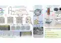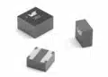


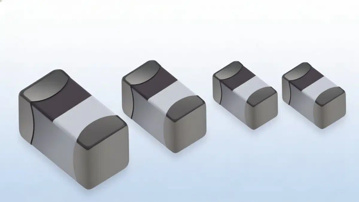
Bourns has released four new multilayer chip inductor series – CE0603G, CE0603M, CE1005Q and CE1608Q – aimed at compact RF and wireless applications where footprint, high‑frequency performance and reliability are critical.
The families span very small 0603 metric up to 1608 metric sizes and cover inductance values from sub‑nanohenry up to hundreds of nanohenry, giving design engineers a broad choice for matching, filtering and decoupling in modern communication hardware.
Key features and benefits
These multilayer SMD chip inductors use a monolithic construction that is designed to deliver stable electrical performance and robust mechanical reliability in miniature SMD packages.
Key characteristics across the four series include:
- Monolithic multilayer construction for high reliability in reflow‑soldered SMT assemblies.
- Magnetically shielded design to reduce radiated magnetic fields and minimize coupling into adjacent sensitive traces or components.
- Compact footprints with low profiles, max. 0.8 mm height, suitable for dense smartphone‑class and module‑level layouts.
- High self‑resonant frequency (SRF) values up to 20,000 MHz depending on value and series, supporting RF signal paths into the GHz range.
- Inductance ranges from 0.3 nH up to 470 nH depending on series, covering impedance matching, RF choke and general filter applications.
- DC resistance ranges from 0.05 Ω to 10 Ω according to the manufacturer datasheet, supporting both low‑loss RF paths and higher value parts where series resistance is less critical.
- Rated current capability from 100 mA up to 1,000 mA, enabling use in low‑voltage power supply modules and bias networks.
- Operating temperature range from −55 °C to +125 °C, compatible with many industrial and automotive‑style environments where extended temperature is required.
- RoHS compliant, in line with Directive 2015/863.
In practice, the combination of small size, shielded construction and high SRF makes these parts attractive when designers need controlled inductance at RF frequencies without sacrificing PCB density or EMC performance.
Typical applications
Bourns specifically targets these multilayer chip inductors at RF and high‑frequency signal chains, but the electrical characteristics also lend themselves to a broad set of low‑voltage and wireless systems.
Typical application areas include:
- RF and wireless communication front‑ends, for matching networks, RF chokes and inter‑stage filtering.
- RF amplifiers, where high SRF and low DCR help maintain gain and noise performance.
- Radio transmitters, including VHF/UHF and higher‑frequency radios using compact SMD matching components.
- Radar modules, where small, shielded inductors help with filter and matching functions in space‑constrained layouts.
- Noise filters in mixed‑signal and RF boards, combining these inductors with capacitors in LC filters.
- Low‑voltage power supply modules, for small bias chokes and local filtering in DC/DC converters or LDO bias networks.
- Various mobile electronic devices, such as smartphones, tablets, wearables and wireless modules, where footprint and height are tightly constrained.
For purchasing and project engineers, the wide operating temperature range and shielded construction are important when qualifying components for use in more demanding embedded and communication equipment.
Technical highlights
The four series share the same general multilayer, shielded technology but differ in size and inductance coverage. This allows engineers to trade footprint and height against inductance range, SRF and DCR.
Series overview
| Series | Size (L × W × H, mm) | Inductance range (nH) | SRF range (MHz) | DCR range (Ω) | Rated current (mA) | Operating temperature (°C) |
|---|---|---|---|---|---|---|
| CE0603G | 0.6 × 0.3 × 0.3 | 0.3 – 39 | 1,500 – 18,000 | 0.07 – 2.4 | 120 – 850 | −55 to +125 |
| CE0603M | 0.6 × 0.3 × 0.3 | 0.6 – 75 | 1,000 – 20,000 | 0.07 – 10 | 100 – 850 | −55 to +125 |
| CE1005Q | 1.0 × 0.5 × 0.5 | 0.3 – 150 | 550 – 10,000 | 0.08 – 3.2 | 140 – 1,000 | −55 to +125 |
| CE1608Q | 1.6 × 0.8 × 0.8 | 1 – 470 | 300 – 10,000 | 0.05 – 2.6 | 150 – 1,000 | −55 to +125 |
What the key specs mean in practice
- High SRF: The specified SRF values up to 20 GHz indicate that the inductors behave predominantly inductively across a wide RF band before parasitic capacitance dominates. This is important in matching networks and RF filters, where a low SRF can severely limit usable frequency range.
- Low DCR: Lower DCR reduces insertion loss and improves efficiency, especially in RF chokes carrying DC bias current and in low‑voltage supply filters.
- Rated current: The current ratings indicate the maximum DC current before significant self‑heating or inductance shift. For bias chokes and small power inductors in RF modules, this helps ensure thermal and electrical stability under operating load.
- Small footprint and profile: The 0603 metric series at only 0.3 mm height and the 1608 series at 0.8 mm height allow use in very thin modules, stacked boards or under shielding cans where keep‑out height is restricted.
Design‑in notes for engineers
When designing these multilayer chip inductors into RF or mixed‑signal circuits, a few practical considerations can help achieve predictable performance:
- Select the series by footprint and inductance range:
- Use CE0603G or CE0603M when absolute minimum footprint and height are required in very compact modules.
- Use CE1005Q when a slightly larger pad area is acceptable for easier routing, soldering and inspection.
- Use CE1608Q when higher inductance values up to 470 nH are needed, for example in low‑frequency filters or bias chokes.
- Check SRF against your operating frequency:
- Choose values where the SRF is comfortably above the highest frequency of interest so that the inductor still behaves dominantly inductively.
- Verify DCR and current rating:
- Ensure the DCR is low enough to meet insertion loss and efficiency targets.
- Confirm that the rated current exceeds the maximum DC bias in your application, with appropriate derating for ambient temperature and self‑heating.
- Consider EMC and layout:
- The magnetically shielded construction helps reduce coupling to nearby circuits, but good RF layout practice remains essential.
- Place inductors close to associated components (capacitors, active devices) to minimize lead length and stray inductance.
- Soldering and reliability:
- The monolithic construction is designed for SMT reflow processes; follow Bourns’ recommended reflow and handling guidelines from the datasheet for long‑term reliability.
- Qualification:
- For safety‑critical or automotive‑like environments, combine the information in this product bulletin with full datasheet specifications and any available reliability or AEC‑Q‑related documentation before release to production.
For purchasing and component engineering teams, aligning on a preferred size family (for example, standardizing on 1005 or 1608 metric for RF inductors) can simplify PCB library management and reel handling while still using the same Bourns CE series technology.
Source
The information in this article is based on a new product release bulletin published by Bourns for the CE0603G, CE0603M, CE1005Q and CE1608Q multilayer chip inductor series, supplemented by manufacturer product documentation as referenced below.