


This presentation from Würth Elektronik by Ashiro Chen and Iván Arias provides characterization and selection of common mode choke parameters for DC and Data/Signal Lines to optimize the RF circuits for compliance as RF Circuit Design for Next-Generation Communication Systems.
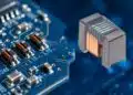
Common Mode Chokes (CMCs) are indispensable components for effective noise suppression and maintaining signal integrity in a wide array of electronic designs.
Their proper selection and application are critical for ensuring electromagnetic compatibility (EMC) and overall system performance. This presentation focuses on providing a systematic approach to understanding and utilizing CMCs effectively.
The presentation provides an in-depth look at:
- The characterization of key CMC parameters, including impedance, inductance, rated current, and frequency response, to fully understand their impact on overall system performance.
- A systematic approach to selecting the most suitable CMC based on specific application requirements during the design stage.
- Strategies for ensuring effective noise suppression while simultaneously preserving critical signal and power integrity.
- Discussion of important practical considerations such as the choice of core material, optimal winding configuration, and the effects of saturation to support optimal component selection in various electronic designs.
Key Takeaways
- The presentation from Würth Elektronik focuses on common mode chokes to ensure effective noise suppression and signal integrity.
- Proper selection of common mode chokes (CMCs) impacts electromagnetic compatibility and overall system performance.
- Key aspects include the characterization of CMC parameters and strategies for noise suppression while maintaining signal integrity.
- RF circuit design involves balancing theoretical models, simulations, and compliance with international standards.
- Engineers can leverage optimization techniques to improve development cycles and meet market requirements.
Introduction
This presentation explores the design, optimization, and compliance aspects of RF Circuit Design for Next-Generation Communication Systems. It provides a structured overview of theoretical foundations, practical implementation, and regulatory considerations. The content is tailored for engineers, researchers, and decision-makers seeking both technical depth and actionable insights.
Chapter 1: Fundamentals of RF Circuit Design
RF circuit design requires balancing theoretical models with real-world constraints. The following subsections outline the essential building blocks.
1.1 Transmission Line Theory
At high frequencies, PCB traces behave as transmission lines. The characteristic impedance
depends on distributed inductance (L) and capacitance (C).
1.2 Parasitic Effects
Parasitic capacitance and inductance significantly alter circuit behavior. Table 1 summarizes typical parasitic ranges for common components.
| Component | Parasitic Capacitance (pF) | Parasitic Inductance (nH) |
|---|---|---|
| MLCC (Multilayer Ceramic Capacitor) | 0.1 – 1.5 | 0.5 – 2.0 |
| SMD Resistor | 0.05 – 0.2 | 0.3 – 1.0 |
| Inductor (Wire-wound) | 0.2 – 0.8 | 1.0 – 5.0 |
Chapter 2: Simulation and Optimization
Simulation tools such as ADS, HFSS, or open-source SPICE variants allow engineers to predict performance before prototyping.
2.1 Discrete Optimization
Optimization algorithms can minimize insertion loss or maximize gain. For example, the cost function for impedance matching can be expressed as:
where Z(x) is the impedance of the circuit under optimization and Z₀ is the reference impedance (typically 50 Ω).
2.2 Monte Carlo Analysis
Monte Carlo simulations account for component tolerances. Table 2 illustrates yield predictions for different tolerance levels.
| Tolerance (%) | Predicted Yield (%) |
|---|---|
| ±1 | 95 |
| ±5 | 82 |
| ±10 | 65 |
Chapter 3: Compliance and Standards
RF devices must comply with international standards such as ETSI EN 300 328 (EU) and FCC Part 15 (USA). Non-compliance can result in costly redesigns or market bans.
3.1 EU Regulations
The EU requires conformity assessment and CE marking. Documentation must include test reports, risk analysis, and a Declaration of Conformity.
3.2 International Considerations
Global markets require harmonization with multiple standards. Table 3 compares EU and US requirements.
| Region | Standard | Key Requirement |
|---|---|---|
| EU | ETSI EN 300 328 | Transmit power ≤ 20 dBm |
| USA | FCC Part 15 | Transmit power ≤ 30 dBm |
Conclusion
RF circuit design is a multidisciplinary challenge requiring careful balance between theory, simulation, and compliance. By integrating optimization techniques, accounting for parasitics, and adhering to international standards, engineers can accelerate development cycles and ensure market readiness.
Frequently Asked Questions (FAQ)
The main challenges include managing parasitic effects, ensuring impedance matching, and meeting international compliance standards such as ETSI EN 300 328 and FCC Part 15.
Simulation tools allow engineers to predict circuit performance, optimize discrete components, and reduce costly prototyping cycles by identifying issues early in the design process.
RF devices must comply with regional and international standards. In the EU, ETSI EN 300 328 applies, while in the USA, FCC Part 15 governs RF emissions and transmit power.
How-to: Optimize an RF Circuit for Compliance
- Define Design Requirements
Identify target frequency range, bandwidth, and compliance region (EU, USA, or global).
- Model Transmission Lines
Use transmission line theory to calculate characteristic impedance Z=LC and ensure PCB traces are properly matched.
- Run Simulation and Optimization
Apply discrete optimization and Monte Carlo analysis to account for component tolerances and maximize yield while minimizing insertion loss.
- Validate Against Standards
Compare design results with ETSI EN 300 328 (EU) and FCC Part 15 (USA) requirements, adjusting transmit power and emissions as needed.
- Document and Certify
Prepare compliance documentation, including test reports, risk analysis, and a Declaration of Conformity for CE or FCC certification.