


This article was adapted and edited by a blog post by Pablo Blázquez, Frenetic Power Εlectronics Εngineer discuss the HF Planar Magnetics advantages, challenges, best design practices, ideal applications, and reasons why it’s a game-changer in modern electronics.
Key Takeaways
- High-frequency planar magnetics are crucial in modern electronics due to their compactness and efficiency, especially in AI-driven applications.
- They outshine conventional wound magnetics in high-density power converters, offering benefits like low profile, repeatable designs, and reduced electromagnetic interference.
- Engineers face challenges with heating, skin effect, and material selection, which require careful design practices for optimal performance.
- Planar magnetics serve well in diverse industries such as power electronics, telecommunications, aerospace, medical devices, and data centers.
- This article highlights the importance of using planar magnetics as a design choice in the GaN era, providing guidance on best practices and potential applications.
- Includes a 100 W USB Type‑C planar flyback case study and a 700 W PSFB comparison between conventional PQ and planar EQ transformers using Frenetic tools.
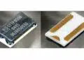
Planar Magnetics – High-Frequency Benefits
High‑frequency planar magnetics are moving from a niche option to a mainstream choice in high‑density power converters driven by AI data centers, servers, telecom and EV infrastructure. As GaN devices push switching frequencies into the 0.5–1 MHz range with 400–650 V buses, the limiting factor is no longer the semiconductor—it is the magnetics, their parasitics and their thermal behavior.
Planar transformers and inductors offer a unique combination of very low profile, tightly controlled leakage inductance and capacitance, and excellent reproducibility in volume production. At the same time, conventional wound magnetics remain highly competitive for rapid prototyping, low‑to‑medium volumes and applications where the mechanical envelope favors taller parts with smaller footprints.
This article provides a practical guide to high‑frequency planar magnetics in the GaN era: where they make sense, how they differ from conventional wound parts, which design constraints dominate above 500 kHz, and what engineers should watch when moving from a PQ‑class wound transformer to an EQ/ER‑class planar solution.
GaN HEMTs in the 400–650 V class can deliver roughly an order of magnitude lower output capacitance‑related charge and essentially zero reverse‑recovery current compared to silicon superjunction MOSFETs, making 0.5–1 MHz LLC and PSFB stages practical with efficiencies in the 96–99% range. In this regime, 1–3% residual losses concentrate in transformers, inductors and EMI chokes, so skin and proximity effects, core losses and parasitics become first‑order design targets rather than afterthoughts.
Planar magnetics are particularly attractive here because their PCB‑defined geometry allows you to deliberately set leakage inductance for ZVS, control primary–secondary capacitance into the tens to low hundreds of picofarads, and maintain repeatable self‑resonant frequencies over production. The same attributes that help you pass EMI at 500 kHz also make GaN‑level MHz operation feasible in real products.
What are the benefits?
HFPM brings an array of benefits to the table, making it a highly desirable choice for different applications. Let’s explore some of these advantages:
- Compact and Lightweight: High-frequency operation allows HFPM to be remarkably smaller and lighter than their low-frequency counterparts. This advantage is a game-changer for applications with limited space or weight constraints.
- Enhanced Efficiency: HFPM exhibits reduced energy losses when compared to low-frequency components. This translates to improved overall efficiency in power conversion systems, which is particularly valuable in energy-conscious industries.
- Minimal Electromagnetic Interference (EMI): Operating at high frequencies inherently results in less electromagnetic interference (EMI). As a result, HFPM is an ideal choice for applications where minimizing EMI is essential, such as medical devices, aviation, and communication equipment.
- Fast Response Time: HFPM offers swift response to changes in input voltage or load conditions. This rapid adjustment capability is invaluable in applications requiring real-time and precise power delivery.
Planar vs. Conventional Magnetics
High‑frequency planar magnetics replace traditional round‑wire windings with flat conductors implemented on a PCB, etched copper foils, or leadframes combined with low‑profile cores. This change in geometry improves window utilization, enables a very low profile, and produces highly repeatable parasitics, which are essential advantages when operating from hundreds of kilohertz up to several megahertz.
Planar and conventional wound magnetics differ in several key geometry design aspects:
| Aspect | Conventional wound parts | Planar magnetics (PCB / foil) |
|---|---|---|
| Winding geometry | Round wire, often randomly layered | Flat copper layers with defined shapes and routing |
| Profile vs. footprint | Higher profile, smaller PCB footprint | Very low profile, usually larger footprint |
| Parasitic predictability | Wider tolerance due to manual winding spread | Well‑controlled by layer stack‑up and artwork |
| Thermal path | Limited contact area to PCB or heatsink | Large copper areas and core faces improve heat spreading |
| Manufacturing variation | Higher variation between units | High repeatability, suited to volume production |
When to Move from Conventional to Planar
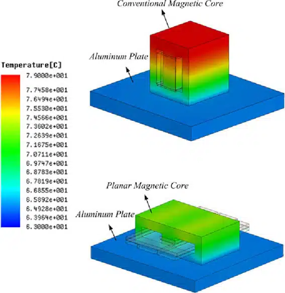
A useful way to decide between wound and planar magnetics is to start from a concrete design, such as a 700 W phase‑shift full‑bridge (PSFB) converter operating from 370–440 VDC to 28 V at around 100 kHz. In this application, a conventional PQ32/35 transformer using round, litz or foil windings is mechanically tall (about 35 mm), relatively heavy and shows higher, less predictable leakage inductance and total losses. A planar alternative based on an EQ38/8/25 core, implemented with PCB windings and a low‑profile PLT stack, reduces height to roughly 10.7 mm, cuts weight by about a factor of three and lowers both total losses and leakage inductance at the cost of greater board footprint.
For early prototypes and low‑to‑medium volume products, PQ‑class wound transformers remain attractive. Cores, bobbins and wire are easy to source, layer order and turns can be reworked in the lab within days, and there is no need to wait for PCB tooling whenever requirements change. In contrast, planar EQ‑class transformers come into their own when production runs reach hundreds of thousands of units, mechanical height is tightly constrained (for example in 1U shelves or compact EV chargers), and reproducible leakage and capacitance are crucial for EMI and resonant behavior. Once the PCB and core stack‑up are frozen, planar magnetics offer excellent lot‑to‑lot repeatability and competitive cost per unit.
The workflow demonstrated with Frenetic AI, Frenetic Simulator and the Planar Design Tool illustrates how to base this choice on quantified data rather than intuition. Starting from the PSFB electrical specifications, Frenetic AI proposes both conventional and planar options; Frenetic Simulator then refines core selection and operating points, and the Planar Design Tool parameterizes window usage, turns distribution, current density, interleaving and parasitic elements using 2D finite‑element analysis. The resulting loss, temperature and leakage figures make it straightforward to compare PQ32/35 and EQ38/8/25 against your mechanical and cost constraints and decide whether the project should stay with a wound transformer or invest in a planar solution.
| Aspect | Conventional PQ32/35 | Planar EQ38/8/25 |
|---|---|---|
| Winding technology | Round / litz / foil on bobbin | PCB windings (planar) |
| Profile (height) | ≈35 mm | ≈10.7 mm |
| Width/depth footprint | Smaller footprint | Larger width and depth |
| Weight | Higher | About 3× lower |
| Total losses (example) | ≈6.1 W | Lower than 6.1 W after optimization |
| Leakage inductance | Higher, more variable | Lower, tightly controlled by interleaving |
| Prototype flexibility | Very high; easy lab rework | Low; PCB change needed for variants |
| High‑volume cost | Higher per unit | Lower per unit once PCB is tooled |
These structural differences are the reason planar magnetics can simultaneously offer compactness, efficiency and predictable EMI performance in modern high‑density power converters.
Challenges of High-Frequency Planar Magnetics
While HFPM has numerous advantages, it also presents some unique challenges that engineers must address:
- Skin Effect: At high frequencies, electrical currents tend to concentrate near the surface of conductors. This phenomenon, known as the skin effect, can increase resistance and reduce the efficiency of HFPM components. Proper design techniques are necessary to mitigate this effect.
- Material Selection: Selecting the appropriate core material for HFPM is crucial. Conventional magnetic materials may not perform optimally at high frequencies, necessitating the use of specialized materials with low core loss and high permeability.
- Parasitic Effects: HFPM components are prone to parasitic capacitance and inductance effects, which can impact their performance. Engineers must carefully consider and mitigate these effects during the design phase.
- Heat Management: High-frequency operation can generate more heat in magnetic components. Effective heat dissipation mechanisms must be integrated into the design to ensure reliability.
Skin and Proximity Effects in Planar Conductors
At high frequency, the current in a copper conductor does not occupy the full cross‑section uniformly, but crowds near the surface (skin effect) and is further pushed toward edges and specific regions by magnetic fields from neighboring conductors (proximity effect). In planar magnetics, where conductors are wide and stacked in parallel layers, these effects can dominate copper loss if not considered early in the design.
Some practical guidelines:
- Prefer several thinner copper layers in parallel over a single very thick layer for the same DC resistance, as this can reduce effective AC resistance.
- Distribute vias along the current path so that parallel layers share current evenly and avoid local hot‑spots.
- Use interleaving patterns that balance low leakage inductance with acceptable AC loss; extremely tight coupling is not always optimal if it greatly increases proximity‑effect losses.
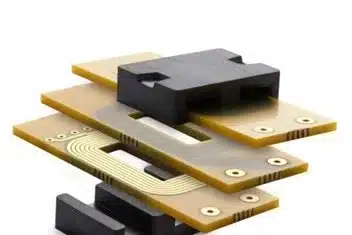
PCB Stack‑Up, Layout and Parasitics
Because planar windings live in the PCB itself, stack‑up definition and layout become primary design tools rather than just routing details.
Leakage inductance, interwinding capacitance, creepage and clearance are all strongly influenced by how layers and copper shapes are arranged.
For practical layout:
- Use broad copper areas for windings when low resistance is important, but introduce spacing or segmentation when you need to reduce capacitance or control current distribution.
- Place primary and secondary layers close for low leakage inductance when regulation and fast response are priorities; insert shielding or spacing layers if common‑mode noise or EMI become problematic.
- Avoid long, narrow “necks” in winding shapes, which concentrate current and increase local losses.
- Keep high‑dv/dt nodes away from sensitive circuitry and consider guard traces or dedicated shield layers connected to quiet reference potentials.
Layout and Stack‑Up Impact Cheat Sheet
The table below summarizes how common planar layout decisions tend to affect key magnetic and EMI parameters at a glance.
| Layout / stack‑up choice | Effect on leakage inductance | Effect on interwinding capacitance | Impact on losses & EMI |
|---|---|---|---|
| Primary and secondary on opposite sides, no interleaving | Higher leakage, weaker coupling | Lower capacitance | Better common‑mode EMI, but worse regulation and transient response |
| Simple interleaving (P–S–P or P–S–S–P) | Lower leakage, stronger coupling | Moderate to higher capacitance | Improved regulation and dynamics, may worsen common‑mode EMI |
| Strong interleaving with multiple sections (P–S–P–S…) | Very low leakage, very strong coupling | High capacitance | Excellent dynamics, but higher CM noise and potential HF losses |
| Wide solid copper windings, minimal spacing | Very low leakage inside a winding | High intra‑winding capacitance | Low DC resistance, higher AC loss and more EMI coupling |
| Segmented / meandered windings | Slightly higher leakage | Lower effective capacitance | Better EMI control, but longer path can increase copper loss |
| Adding shield layer between primary and secondary | Slight increase in leakage | Reduces capacitive coupling to secondary | Helps CM EMI; shield must be carefully referenced to avoid noise paths |
| Increased vertical spacing between windings | Higher leakage | Lower capacitance | Easier EMI control, but worse coupling and potentially higher voltage stress |
| Dense via stitching between parallel layers | Minimal effect on leakage | Minimal direct effect on capacitance | Reduces current crowding and hot spots, lowering AC and DC copper loss |
The Best Design Practices
Now that we’ve explored the benefits and challenges, we can discuss the best practices for designing HFPM. Let’s start with the Skin Effect Mitigation: engineers can employ techniques such as litz wire or foil conductors to minimize the skin effect and ensure optimal current distribution. The material selection is also crucial, and a careful consideration of core materials is essential. Engineers should opt for materials specifically designed for high-frequency applications, ensuring minimal core loss and high permeability.
Parasitic effects reduction needs to be mentioned as well: engineers should employ layout and component placement strategies to minimize parasitic capacitance and inductance. Proper grounding and shielding can also help reduce unwanted effects.
And finally, the Heat control, as an effective heat management is critical for HFPM components. Engineers should integrate heat sinks, thermal vias, and other cooling solutions to prevent overheating and ensure long-term reliability.
Practical Design Flow for Planar Transformers
When moving from concept to an actual HF planar transformer or inductor, a simple design flow helps structure decisions:
- Define electrical requirements
Start from input/output voltages, power level, topology, switching frequency, isolation class, maximum ambient temperature and efficiency target.
From these, derive RMS and peak currents in each winding plus allowable ripple and temperature rise. - Select core family and size
Choose a planar core (for example low‑profile E/ER/EQ types) with sufficient window area for the windings and enough cross‑section to keep flux density within safe limits at your maximum operating frequency.
At HF, core loss becomes a major contributor, so specialized low‑loss materials intended for hundreds of kilohertz and above are preferred. - Determine turns and conductor geometry
Based on the chosen topology and voltage levels, calculate the primary and secondary turns to satisfy both conversion ratio and maximum flux density limits.
Then select copper width, thickness and number of parallel layers such that DC resistance and HF losses (skin and proximity effects) remain acceptable. - Define PCB stack‑up and interleaving
Decide how many PCB layers will carry windings and how they are arranged (for example P–S–P–S or P–S–S–P).
Interleaving can significantly reduce leakage inductance and improve transient response, but may increase interwinding capacitance, which impacts EMI. - Address thermal and mechanical integration
Estimate core and copper losses and map them onto your geometry to predict temperature rise.
Use copper planes, thermal vias and good core‑to‑PCB contact to create effective heat paths, and verify that the component fits mechanical height and clearance constraints.
Case Study: 100 W USB Type‑C Planar Flyback Transformer
A practical example of high‑frequency planar magnetics in production‑class hardware is a 100 W USB Type‑C flyback transformer implemented on an ER41 planar core and designed with Frenetic’s Planar Tool is shown in this article: Designing a USB Type‑C Flyback Planar Transformer with Frenetic’s Planar Tool. The goal is to meet tight height constraints for modern USB‑PD adapters while keeping losses and parasitics under control so that simulations match lab measurements.
In this design, the transformer uses a standard ER41 ferrite geometry in 3C95 material with a single 0.2 mm air gap to set the primary inductance. The primary winding has 21 turns implemented as two parallels across six PCB layers (three layers per parallel), carrying roughly 2.5 A RMS at the design operating point. The secondary has 3 turns, one turn per layer, with about 18 A conduction current, which leads to a hybrid realization: the high‑current secondary uses copper stamps or busbars instead of uneconomical ultra‑thick PCB copper.
Harmonic‑based simulations in the Planar Tool predict a total transformer loss of about 1.6 W at the chosen operating conditions, with primary‑referred leakage inductance around 2.7 µH and lumped primary capacitance about 85 pF. These values translate into a relatively high self‑resonant frequency for a 100 W flyback and give the designer enough leakage for clamp optimization without excessive voltage overshoot. The ability to export a detailed LTspice model that includes magnetizing inductance, leakage and frequency‑dependent loss terms closes the loop between magnetics design and converter‑level verification.
From a system perspective, the ER41 planar transformer demonstrates several of the key benefits discussed earlier in this article. The low profile and PCB‑integrated windings support slim USB‑C adapters and embedded USB‑PD stages on notebook or docking‑station motherboards. Controlled leakage inductance and well‑defined primary capacitance simplify EMI filter design and lower the risk of unpleasant surprises during late‑stage compliance testing. At the same time, the hybrid PCB‑plus‑stamp approach keeps current density in a practical range and allows purchasers to source the PCB and stamped copper from conventional suppliers.
passive-components
For engineers, this example reinforces a few practical lessons. First, planar magnetics scale well into the 60–120 W USB‑C power segment when core, gap and layer arrangement are optimized numerically rather than by trial‑and‑error. Second, explicit modeling of non‑sinusoidal flyback currents via harmonics is essential to avoid underestimating AC copper and core losses. Finally, integrating a tool‑generated transformer macro‑model directly into the flyback simulation allows verification of soft‑switching behavior, snubber networks and control‑loop dynamics with a magnetics model that reflects the intended planar geometry.
passive-components
Safety, Standards and Reliability
For many of the applications you list—especially aerospace, avionics, medical and off‑line power supplies—planar magnetics must satisfy strict safety and reliability requirements.
Designers need to treat the PCB and any auxiliary insulation materials as part of the insulation system, not just as a mechanical support.
Key considerations:
- Verify creepage and clearance distances on the actual PCB artwork against the applicable IEC/UL standards for your voltage and pollution degree.
- Use slots, wider separations, and dedicated insulation layers where necessary to meet reinforced or basic isolation requirements.
- Plan for appropriate qualification tests such as hipot, partial discharge, thermal cycling and, where relevant, vibration and humidity testing to ensure long‑term reliability.
Where to Use High-Frequency Planar Magnetics and Why
HFPM components find their best use in various applications across different industries. First, there’s Power Electronics, where HFPM is a cornerstone in compact, high-efficiency power conversion systems, including DC-DC converters, voltage regulators, and high-frequency power supplies. Its efficiency benefits are crucial in conserving energy and reducing waste heat.
Then, there’s Telecommunications, as the fast response time and reduced EMI of HFPM make it an ideal choice for telecommunications equipment, ensuring reliable and efficient power delivery. We need to also mention Aerospace and Avionics, where HFPM helps minimize interference while providing compact and lightweight solutions in EMI-sensitive environments, like aircraft and satellites.
Medical Devices is another field where High-Frequency Planar Magnetics are highly employed. HFPM’s compact size and EMI reduction are crucial in medical equipment, where reliability, space constraints, and low EMI are paramount. And finally, Data Centers, where high-frequency power supplies benefit from HFPM’s compactness and efficiency, ensuring stable power delivery in data centers and server farms.
Planar magnetics as a GaN‑era design tool
- Above about 0.5 MHz and 400–650 V, GaN devices move the main design bottleneck from the switches into the magnetics, making core loss, AC copper loss and parasitics central constraints.
- Planar transformers and inductors respond well to this challenge by offering low profile, well‑controlled leakage and capacitance, and high repeatability, especially attractive in AI data center, server and telecom power stages.
- Conventional wound transformers remain the most pragmatic option for fast prototypes, small‑to‑medium volumes and mechanically tall but compact footprints, such as PQ32/35‑class parts in 700 W PSFB converters.
- In high‑frequency GaN designs, designers must start from geometry and PCB layout rather than treating magnetics as a late‑stage black‑box component, explicitly specifying targets for leakage, primary–secondary capacitance and self‑resonant frequency.
- Tool‑assisted workflows (such as Frenetic AI, Simulator and Planar Design Tool) make it practical to compare conventional and planar options early, optimize core and winding choices for 0.5–1 MHz, and base the final selection on quantified losses, parasitics, thermal behavior and manufacturing constraints instead of intuition.
Taken together, these points position high‑frequency planar magnetics not as a universal replacement for wound transformers, but as a powerful, geometry‑driven option that lets engineers fully exploit GaN’s potential when the application, volume and mechanical envelope justify the investment.
Conclusion
High‑frequency planar magnetics have evolved from a niche curiosity into a key enabler for compact, efficient power stages in the GaN era, particularly above about 0.5 MHz and in the 400–650 V range. By deliberately shaping geometry, PCB stack‑up and layer interleaving, designers can turn leakage inductance, interwinding capacitance and thermal behavior from annoying side effects into controlled design parameters.
Planar transformers and inductors are not a universal replacement for conventional wound magnetics, but a powerful option when low profile, tight parasitic control, high repeatability and high‑volume manufacturability are critical, such as in AI data centers, servers, telecom equipment and advanced industrial supplies. Wound PQ‑class parts still shine for rapid prototyping, small‑to‑medium volumes and mechanically taller but footprint‑efficient designs.
The practical workflows, layout guidelines and “when planar vs conventional” insights in this article are intended to help you make that choice with quantified trade‑offs instead of intuition alone. If you are planning a new high‑frequency GaN or Si‑based converter and want to explore planar options, tools and design support from specialists like Frenetic can accelerate the transition from a working prototype to an optimized planar solution.
The case studies and tool‑assisted workflows referenced above provide concrete templates you can adapt when deciding if and how to adopt planar magnetics in your own converters.
Frequently Asked Questions on Planar Magnetics
High-frequency planar magnetics are transformers and inductors that use flat PCB or foil windings with low-profile cores, optimized for operation from hundreds of kilohertz up to the megahertz range. They are designed to offer compact size, controlled parasitics and high efficiency in modern power converters.
Conventional transformers use round wire wound around a bobbin, resulting in taller parts with more variation in leakage inductance and capacitance. Planar magnetics replace round wire with flat PCB or foil windings, giving a much lower profile, predictable parasitics and better thermal paths at the cost of a larger PCB footprint.
Planar magnetics make the most sense in high-density, high-frequency designs where low profile, tight parasitic control and reproducible performance are critical, such as AI data centers, servers, telecom and advanced industrial power supplies. Conventional wound magnetics remain very practical for fast prototyping, small-to-medium volumes and applications that can accept taller components with smaller footprints. This article includes a 100 W USB‑C flyback and a 700 W PSFB example that illustrate how tool‑assisted workflows compare conventional and planar options in practice.
GaN devices allow efficient switching in the 0.5–1 MHz range with 400–650 V buses, shifting the main design bottleneck from semiconductors to magnetics. In this regime, planar magnetics help manage core and copper losses, leakage inductance, interwinding capacitance and thermal behavior so that designers can fully exploit GaN’s speed and efficiency.
Key advantages include compact and low-profile construction, high power density, reduced electromagnetic interference, repeatable parasitics and efficient heat spreading through large copper and core surfaces. These benefits are especially valuable in space-constrained and thermally demanding systems.
Designers must manage skin and proximity effects, select suitable high-frequency core materials, control parasitic capacitance and leakage inductance, and ensure effective heat management. Safety, creepage, clearance and long-term reliability requirements must also be addressed in the PCB layout and insulation system.
Planar magnetics are well suited to power electronics, telecommunications, aerospace and avionics, medical devices and data centers. In these sectors they support compact, low-EMI, high-efficiency power stages with strict mechanical and regulatory constraints including USB Type‑C / USB‑PD adapters around the 60–120 W range, where low profile and repeatable parasitics are critical.
No. Planar magnetics complement rather than replace conventional wound transformers. They are the better choice when high frequency, low profile, tight parasitic control and high-volume manufacturing are priorities, while conventional parts remain attractive for cost-sensitive, lower-volume or mechanically tall designs.
How to design a high-frequency planar transformer
- Step 1 – Define electrical requirements
List input and output voltages, power level, converter topology, switching frequency, isolation class, ambient temperature range and efficiency targets. From these values derive RMS and peak currents in each winding and the allowable temperature rise.
Clear electrical specifications determine flux density limits, current densities and loss budgets, which are fundamental to selecting a suitable core and copper geometry. - Step 2 – Select core family and size
Choose a low-profile planar core (for example E, ER or EQ types) with enough window area for the windings and sufficient cross-sectional area to keep flux density within safe limits at your maximum operating frequency. Specialized magnetics design tools can automate this step by proposing suitable planar and conventional options based on your electrical specifications.
At high frequency, core losses increase quickly, so using a dedicated high-frequency material and a correctly sized core is critical for efficiency and thermal performance. - Step 3 – Determine turns and conductor geometry
Calculate the primary and secondary turns based on the converter topology and voltage levels to satisfy both conversion ratio and maximum flux density constraints. Then choose copper width, thickness and number of parallel layers so that DC resistance and AC losses from skin and proximity effects remain acceptable.
Turns and conductor dimensions set both electrical performance and loss distribution, directly impacting efficiency, temperature rise and regulation. - Step 4 – Define PCB stack-up and interleaving
Decide how many PCB layers will carry windings and how they will be arranged, for example simple P–S–P interleaving or more complex multi-section patterns. Adjust vertical spacing, shielding layers and segmentation to control leakage inductance and interwinding capacitance.
PCB stack-up and interleaving are the main tools for tuning coupling, EMI behavior and self-resonant frequencies in planar magnetics. - Step 5 – Address thermal and mechanical integration
Estimate core and copper losses, then map them onto the physical geometry to predict temperature rise. Use wide copper planes, stitched thermal vias and solid core-to-PCB contact, and check that the assembly fits height, footprint and creepage and clearance constraints.
Thermal and mechanical design ensures that the planar transformer can operate safely and reliably in the target environment while meeting the required power density. - Step 6 – Verify safety, standards and reliability
Check creepage and clearance distances on the actual PCB artwork against the relevant IEC and UL standards. Include any necessary slots, insulation layers, coatings or potting compounds, and plan qualification tests such as hipot, partial discharge and thermal cycling.
Treating the PCB and insulation system as part of the transformer ensures long-term reliability and regulatory compliance in applications such as off-line supplies, medical, avionics and industrial equipment.
References
- Planar Magnetics – Benefits, Design Practices and When They Make Sense
- Designing a USB Type‑C Flyback Planar Transformer with Frenetic’s Planar Tool. – 100 W ER41 planar flyback case study using Frenetic Planar Tool.
- From Conventional to Planar Transformer: When It Make Sense. – 700 W PSFB PQ32/35 vs EQ38/8/25 comparison using Frenetic AI, Simulator and Planar Design Tool.