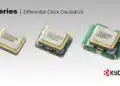


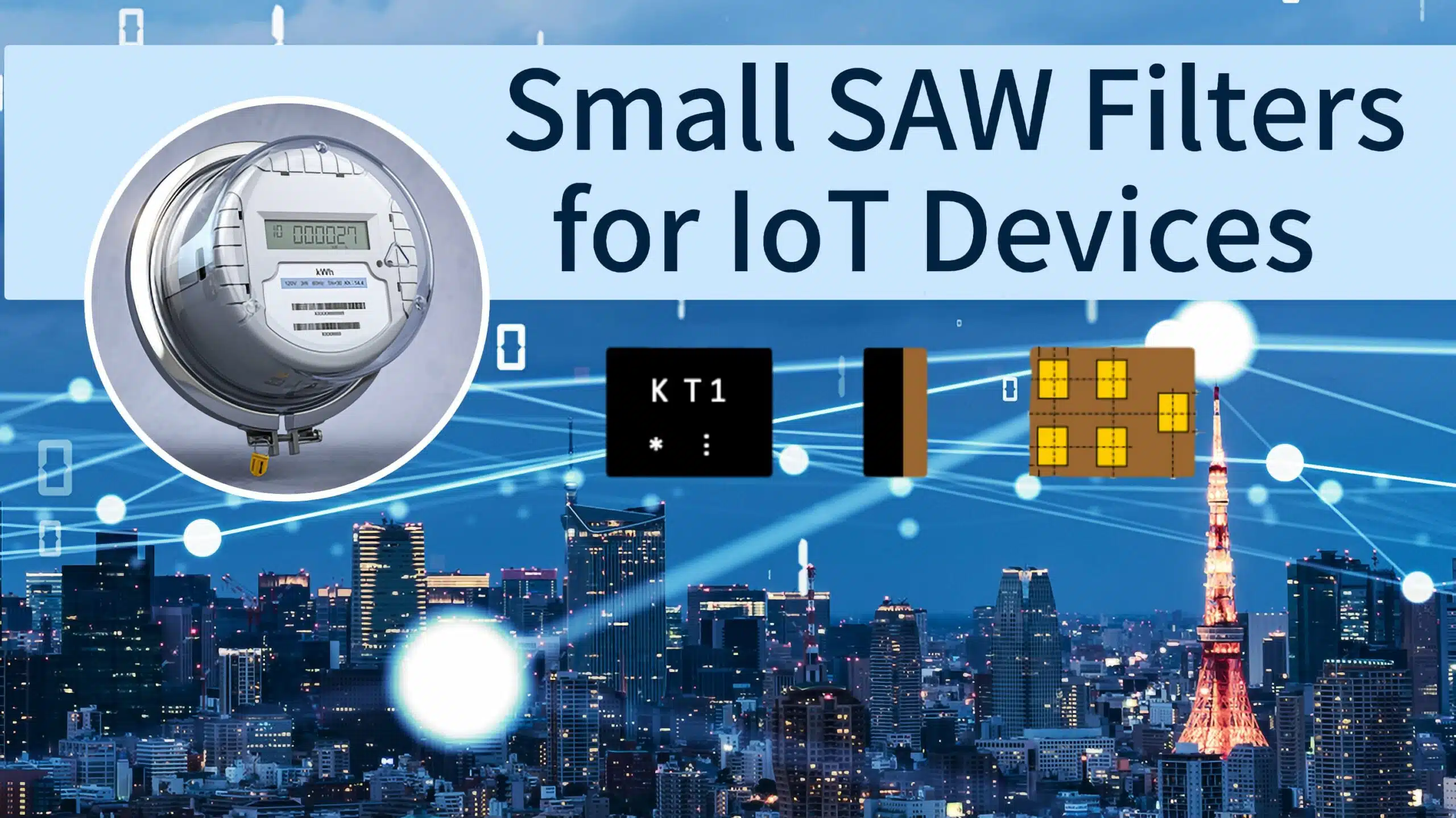
Kyocera has introduced a family of compact SAW (Surface Acoustic Wave) filters optimized for low‑power wireless communication in IoT devices such as smart meters and compact wireless modules.
These devices target popular ISM and sub‑GHz bands, helping designers meet coexistence, size and power constraints in dense RF environments. For engineers, the series offers a way to shrink RF front‑ends while maintaining selectivity and robust operation over a wide temperature range.
Role of SAW filters in IoT RF front‑ends
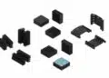
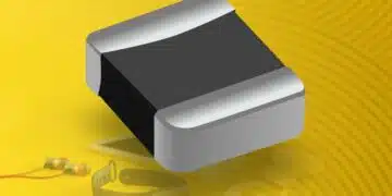
In typical IoT nodes, especially smart meters and similar infrastructure devices, the RF front‑end must handle narrowband communication in crowded spectrum, often next to cellular, Wi‑Fi or other ISM services. SAW band‑pass filters provide the necessary channel selectivity between the antenna and the transceiver or PA/LNA. They attenuate out‑of‑band interferers, improve receiver sensitivity and ease EMC compliance, all in a small SMD package that fits densely populated RF PCBs.
Kyocera’s small SAW filters for IoT are designed specifically for these compact RF sections, where PCB area and height are limited but stable RF characteristics over temperature and time are still required.
Key features and benefits
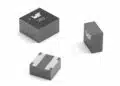
Kyocera’s IoT‑oriented SAW filters emphasize a combination of compact size, RF performance and robust environmental characteristics suitable for long‑life field installations.
Key characteristics include:
- Small surface‑mount packages suitable for high‑density IoT modules and smart meter RF boards.
- Center frequencies matched to common IoT bands as specified in the manufacturer datasheet (e.g. sub‑GHz smart‑metering bands and 2.4 GHz‑class ISM, depending on the specific part number).
- Low insertion loss to maintain receiver sensitivity and minimize PA output power, supporting low‑power operation and extended battery life.
- High out‑of‑band attenuation to suppress adjacent‑channel and blocker signals, improving coexistence with nearby wireless standards.
- Temperature‑stable filter characteristics according to the specified operating temperature range and technology used (including temperature‑compensated SAW structures on selected parts).
- Surface‑mount construction compatible with standard lead‑free reflow soldering and automated assembly.
For purchasing and component engineering, the combination of standardized SMD outlines and clearly specified RF characteristics simplifies second‑source evaluation and long‑term lifecycle planning.
Typical applications
Kyocera positions these small SAW filters primarily for IoT and smart infrastructure devices where compact RF modules are embedded into constrained housings.
Typical end‑equipment includes:
- Smart meters for electricity, gas and water, including RF boards integrated into metering heads or communication modules.
- Industrial IoT nodes using licensed or unlicensed narrowband RF links for telemetry and remote monitoring.
- Compact RF modules and communication plug‑ins that OEMs integrate into larger host systems (appliances, building automation, industrial controllers).
- Other battery‑powered sensors and actuators requiring robust sub‑GHz or ISM‑band connectivity in crowded RF environments.
In these designs, the SAW filter is usually placed between the antenna matching network and the RF transceiver or LNA/PA, providing band selection and protecting the receiver from out‑of‑band power.
Technical highlights
From a circuit‑design perspective, the important parameters of these SAW filters are their center frequency, bandwidth, insertion loss, return loss, attenuation profile and power handling, all of which are defined per part number in the Kyocera datasheet.
Relevant technical aspects include:
- Package dimensions and land patterns designed for compact RF PCBs in IoT modules; exact sizes are according to the manufacturer datasheet for the selected part number.
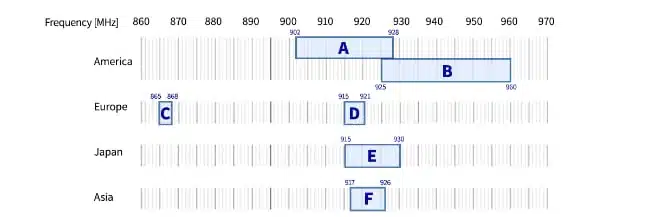
- Defined passband frequency range and nominal center frequency matched to the target regional IoT standard.
- Specified maximum insertion loss in the passband, which directly impacts link budget. Lower insertion loss means less margin consumed by the filter and potentially lower transmit power for the same range.
- Out‑of‑band attenuation curves around the passband, which define how well the filter rejects interferers from neighboring services. This affects coexistence performance in multi‑standard environments.
- Operating temperature range and temperature dependence of center frequency and insertion loss, important for outdoor smart meters or industrial deployments subject to wide thermal swings.
Engineers should always refer to the official Kyocera datasheet for exact numeric values (frequency masks, insertion loss, attenuation at specific offsets and power ratings) when completing RF budget and coexistence calculations.
Design‑in notes for engineers
To get the expected performance from these SAW filters in real hardware, RF layout and system‑level considerations are critical.
Practical design‑in guidelines include:
- Place the SAW filter as close as possible to the RF transceiver or LNA/PA and to the antenna matching network, minimizing series line length and discontinuities.
- Follow Kyocera’s recommended PCB land pattern, including ground via placement, to achieve the specified impedance environment.
- Use controlled‑impedance microstrip or coplanar lines between antenna, filter and RF transceiver to avoid unintended reflections and bandwidth narrowing.
- Take into account the filter’s group delay and insertion loss in the overall link budget and timing analysis, particularly for narrowband or time‑sensitive protocols.
- Simulate the complete RF front‑end, including antenna, matching network and SAW filter S‑parameters provided by Kyocera, to validate coexistence and blocking performance.
- Consider temperature behavior and mounting conditions (enclosure, nearby metal, shielding cans) to ensure that the filter meets specification in the final product environment.
For long‑life infrastructure deployments like smart meters, it is also advisable to review regional frequency bands (see below),
long‑term reliability data, environmental test results and any application notes that Kyocera provides for SAW filters in utility metering and similar applications.
| Part Number | Size | Band Range | Frequency | Type | Production Status |
|---|---|---|---|---|---|
| SF14-0915M5UUP1 | 1.4×1.1 mm | 902–928 MHz | A, D | Standard | In Mass Production |
| SF14-0915M5UUB1 | 1.4×1.1 mm | 902–928 MHz | A, D | Low Loss | In Planning |
| SF14-0925M5UUP1 | 1.4×1.1 mm | 920–930 MHz | E, F | Standard | In Mass Production |
| SF14-0925M5UUC1 | 1.4×1.1 mm | 922–928 MHz | E, F | Low Loss | In Mass Production |
| SF14-0869M5UUB1 | 1.4×1.1 mm | 863–870 MHz | C | Low Loss | In Planning |
| SF14-0942M5UUB1 | 1.4×1.1 mm | 925–960 MHz | B | Standard | In Planning |
Source
This article is based on technical information and product descriptions published by Kyocera for its small SAW filters for IoT devices, adapted and expanded for design and component engineers.