Passive Components Blog
No Result
View All Result
  • Home
  • NewsFilter
    • All
    • Aerospace & Defence
    • Antenna
    • Applications
    • Automotive
    • Capacitors
    • Circuit Protection Devices
    • electro-mechanical news
    • Filters
    • Fuses
    • Inductors
    • Industrial
    • Integrated Passives
    • inter-connect news
    • Market & Supply Chain
    • Market Insights
    • Medical
    • Modelling and Simulation
    • New Materials & Supply
    • New Technologies
    • Non-linear Passives
    • Oscillators
    • Passive Sensors News
    • Resistors
    • RF & Microwave
    • Telecommunication
    • Weekly Digest

    Transformer Design Optimization for Power Electronics Applications

    Microhardness — the Hidden Key to Understanding MnOx Cathode Quality in Tantalum Capacitors

    Samsung to Invest in its Philippine MLCC Facility to Meet Automotive Demand

    Lightweight Model for MLCC Appearance Defect Detection

    DMASS Reports First Positive Signs of European Distribution Market in Q3/25

    TAIYO YUDEN Releases 22uF MLCC in 0402 Size for AI Servers

    Wk 44 Electronics Supply Chain Digest

    Bourns Releases High Current Metal Alloy-based, Multilayer Power Chip Inductors

    Smiths Interconnect Extends Space-Qualified, High-Reliability Fixed Chip Attenuators 

    Trending Tags

    • Ripple Current
    • RF
    • Leakage Current
    • Tantalum vs Ceramic
    • Snubber
    • Low ESR
    • Feedthrough
    • Derating
    • Dielectric Constant
    • New Products
    • Market Reports
  • VideoFilter
    • All
    • Antenna videos
    • Capacitor videos
    • Circuit Protection Video
    • Filter videos
    • Fuse videos
    • Inductor videos
    • Inter-Connect Video
    • Non-linear passives videos
    • Oscillator videos
    • Passive sensors videos
    • Resistor videos

    Transformer Design Optimization for Power Electronics Applications

    Common Mode Chokes Selection for RF Circuits in Next-Generation Communication Systems

    Capacitor Self-balancing in a Flying-Capacitor Buck Converter

    How to Select Ferrite Bead for Filtering in Buck Boost Converter

    Power Inductors Future: Minimal Losses and Compact Designs

    Percolation Phenomenon: Degradation of Molded Power Inductors in DC/DC Converters

    Connector PCB Design Challenges

    Efficient Power Converters: Duty Cycle vs Conduction Losses

    Ripple Steering in Coupled Inductors: SEPIC Case

    Trending Tags

    • Capacitors explained
    • Inductors explained
    • Resistors explained
    • Filters explained
    • Application Video Guidelines
    • EMC
    • New Products
    • Ripple Current
    • Simulation
    • Tantalum vs Ceramic
  • Knowledge Blog
  • Suppliers
    • Who is Who
  • PCNS
    • PCNS 2025
    • PCNS 2023
    • PCNS 2021
    • PCNS 2019
    • PCNS 2017
  • Events
No Result
View All Result
Passive Components Blog
No Result
View All Result

Murata is Looking for Partners to Develop Applications of its New Transparent and Bendable Conductive Film

28.12.2022
Reading Time: 5 mins read
A A

Murata is seeking partners to develop applications for a new transparent and bendable conductive film which combines transparency, flexibility and high conductivity.

Murata Manufacturing is now developing a new material with unprecedented strong points. This new material combines transparency, flexibility, conductivity, and safety.

RelatedPosts

Murata Expands Automotive Metal Frame Y2/X1 Safety MLCC Capacitors to 500V

Murata Opens EMC Test Lab in Nuremberg to Enhance Automotive Support

Murata Integrates Component Models into Cadence EDA Tools

Furthermore, it realizes high workability to be able to easily draw circuit patterns and other elements with diverse methods.

It is possible that we will be able to create new value with approaches different from conventional technologies for electrical and electronic devices by applying this new material. Murata is seeking partners to discuss the application of new ideas using this new material regardless of your business or industry.

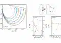
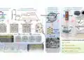
There are broadly two strong points to Transparent and Bendable Conductive Film: it enhances the functions and performance in applications and it produces usage benefits to user companies that develop and produce products to which this material is applied (Fig. 1). 

Fig. 1: Transparent and Bendable Conductive Film Developed by Murata and Its Strong Points

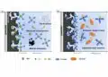
The film combines conductivity while being transparent even when it is bent. Films of indium tin oxide (ITO)-based materials used in touch-panel electrodes, wiring, and other components and conductive films using graphene composite material ink also serve as transparent and bendable conductive films. (Fig.2).

Looking only at transparency, flexibility, and conductivity, there are many materials that display even better characteristics and there are materials that combine two out of three of these strong points. However, it is not easy to find materials that combine these three strong points at a high level like with Transparent and Bendable Conductive Film.

The Film is a hydrophilic material. Accordingly, it can be easily and uniformly dispersed in solvents. Therefore, it is possible to produce inks according to the processing method and to use existing coating and printing techniques to form films with stable characteristics.

Fig. 2: Comparison of the Bending Resistance of Transparent and Bendable Conductive Film and Existing Conductive Films

Specifically, it is possible to draw patterns under normal temperatures and pressures with inkjet printers, stamp and screen printing, spray coating, pen drawing, and other methods. Of course, it will also be possible to open up unknown applications by developing new never-before-seen ground-breaking coating systems and optimizing the ink. The ability to draw patterns using such diverse processing methods is a strong point that will support expansion of applications. For example, it is possible to draw wiring with fine line widths of several hundred microns by using an inkjet printer. Using such processing methods allows patterns to be drawn as desired without a removal process like masks or etching.

In addition, it is possible to draw just the parts that function as conducting wire. Therefore, it also realizes the effective use of materials and a reduction in the environmental burden. On the other hand, adopting a method of coating with a spray means it is even possible to cover substrates with three-dimensional curved surfaces by using the same method as that of coating the body of an automobile.

That enables the formation of conductive film on the surface of large and complex objects. Furthermore, it is also possible to easily add electrical functions to the surface of tools and devices for which the shape itself has meaning.

ITO-based electrodes require some kind of high-temperature treatment to form wiring patterns and similar to exhibit conductivity. For instance, it is necessary to attach film to the substrate with a vacuum deposition process that is performed under a high-temperature and vacuum environment for ITO-based materials.

As a result, it has been impossible to avoid an increase in the processing workload and a deterioration of the substrates to be coated. That led to drawbacks including limited applications and increased costs. Transparent and Bendable Conductive Film does not have such factors hindering an expansion in applications.

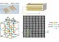
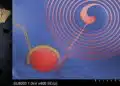
Another major advantage is the fact that post-processing after the pattern formation is simple (Fig.3.). It is necessary to add a firing process at 150 to 200°C for Ag ink that is one of the conventional materials to form transparent conductive film.

Fig. 3: Transparent and Bendable Conductive Film Manifests Conductivity with Just a Low-temperature Process

This is to ensure conductivity by connecting fine Ag particles to each other after drawing the pattern. Transparent and Bendable Conductive Film can demonstrate conductivity just by drying water at 50 to 100°C. Therefore, it is also possible to form it on substrates vulnerable to heat damage. You can even use it with natural drying if you don’t mind waiting for some time.

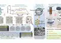
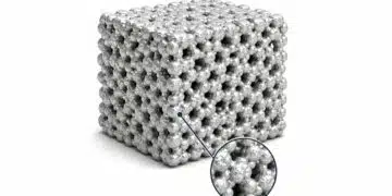
Transparent and Bendable Conductive Film is made from micro-ceramics at the nanometer level with the property to carry electricity. The shape of these micro-ceramics is flat. Accordingly, due to the microscopic size and shape of these ceramics, this material exhibits characteristics halfway between metal and ceramics to obtain transparency and conductivity.

Its workability is also due to this size and shape. The film after coating and drying the ink in which this material is dispersed enters a state in which the entire pattern drawn is energized because the micro-ceramics lie on top of each other. Substances have been emerging in recent years that exhibit unique characteristics due to their nano-sized micro-structure and size instead of the composition of their materials like graphene, which demonstrates high conductivity by connecting carbon (C) atoms.

No rare metals or earths are used. Accordingly, the raw materials are inexpensive and can be stably procured.

In addition, there is room for further adjustments to improve the new material’s characteristics and to enhance its suitability for specific applications by optimizing the composition, structure, and size of the micro-ceramics.

Related

Source: Murata

Recent Posts

Lightweight Model for MLCC Appearance Defect Detection

3.11.2025
9

High Energy Density Polymer Film Capacitors via Molecular and Interfacial Design

15.10.2025
41

Enhancing Energy Density in Nanocomposite Dielectric Capacitors

9.10.2025
46
a Schematic diagram of the BNT-based components constructed based on the entropy-increase strategy. b Digital photograph, cross-sectional SEM image, and EDS mappings of the MLCCs. c Unipolar P-E loops of MLCCs as a function of applied E. d Wrec and η of the MLCCs as a function of applied E. The comparison of (e) Wrec and η, (f) η and UF of the MLCCs with those of other recently reported state-of-the-art MLCCs. source: Nature Communications

Researchers Proposed Enhanced Energy Storage MLCC

1.10.2025
27

Development of Nitrogen-Doped Graphene Supercapacitors 

30.9.2025
19

Researchers Developed Reduced Graphene Oxide (rGO) High Energy Density Graphene Supercapacitors

18.9.2025
41

Researchers Enhanced 2D Ferromagnets Performance

16.9.2025
9

Researchers Demonstrated HfO Anti-Ferroelectric Flexible Capacitors

19.8.2025
21

Additive Manufacturing of Mn-Zn Ferrite Planar Inductors

4.8.2025
46

Researchers Presents High-Performance Carbon-Based Supercapacitors

1.8.2025
45

Upcoming Events

Nov 4
November 4 @ 12:00 - November 6 @ 14:15 EST

Wirebond Materials, Processes, Reliability and Testing

Nov 6
14:30 - 16:00 CET

Self-healing polymer materials for the next generation of high-temperature power capacitors

Nov 11
17:00 - 18:00 CET

Industrial Applications Demand More from Interconnects in Next-Gen Designs

View Calendar

Popular Posts

  • Buck Converter Design and Calculation

    0 shares
    Share 0 Tweet 0
  • Boost Converter Design and Calculation

    0 shares
    Share 0 Tweet 0
  • LLC Resonant Converter Design and Calculation

    0 shares
    Share 0 Tweet 0
  • Flyback Converter Design and Calculation

    0 shares
    Share 0 Tweet 0
  • Ripple Current and its Effects on the Performance of Capacitors

    3 shares
    Share 3 Tweet 0
  • MLCC and Ceramic Capacitors

    0 shares
    Share 0 Tweet 0
  • Dual Active Bridge (DAB) Topology

    0 shares
    Share 0 Tweet 0
  • What is a Dielectric Constant and DF of Plastic Materials?

    4 shares
    Share 4 Tweet 0
  • SEPIC Converter Design and Calculation

    0 shares
    Share 0 Tweet 0
  • Flying Capacitors

    0 shares
    Share 0 Tweet 0

Newsletter Subscription


Passive Components Blog

© EPCI - Leading Passive Components Educational and Information Site

  • Home
  • Privacy Policy
  • EPCI Membership & Advertisement
  • About

No Result
View All Result
  • Home
  • Knowledge Blog
  • PCNS

© EPCI - Leading Passive Components Educational and Information Site

This website uses cookies. By continuing to use this website you are giving consent to cookies being used. Visit our Privacy and Cookie Policy.
Go to mobile version