Silicon based capacitors are typically single MIM (metal-insulator-metal) or a multiple MIM structure electrostatic capacitors build by semiconductor technologies.
Silicon dielectrics are either silicon dioxide (MIS) or silicon nitride (MOS) insulating layers, however semiconductor manufacturing techniques such as atomic layer deposition (ALD) can be used to form other dielectric materials on top of silicon substrate. High density silicon based capacitors are using 3D nano-structured electrodes to achieve higher surface area and thus higher capacitance value.
Key Takeaways
- Silicon capacitors utilize silicon dioxide or silicon nitride dielectrics and offer high stability, reliability, and miniaturization suitable for harsh environments.
- They exhibit strengths like high temperature stability up to 250°C, low leakage current, and long lifetimes but have a limit on maximum capacitance.
- Advanced techniques like 3D nano-structured electrodes and atomic layer deposition (ALD) enhance performance and efficiency in silicon capacitors.
- Though they offer superior performance, silicon capacitors are more expensive than traditional options like MLCCs, limiting their use in certain applications.
- High-density silicon capacitors achieve low losses and improved volumetric efficiency, making them ideal for specialized fields like automotive, aerospace, and military applications.
Introduction
Silicon-based dielectrics such as silicon dioxide and silicon nitride are commonly used in high-density capacitors. Capacitors with silicon dielectrics are ideal for applications that demand high stability, reliability, and tolerance to high temperatures. The performance characteristics of these capacitors make them a suitable choice for use in harsh environment applications. The following are the key strengths and limitations of silicon-based dielectrics.
What Are Silicon Capacitors in the Capacitor Landscape
Silicon-based capacitors are electrostatic capacitors fabricated using semiconductor processes, typically as metal–insulator–metal (MIM) or MOS/MIS structures on a silicon substrate. In contrast to conventional discrete capacitors such as MLCCs or film capacitors, they are closely integrated with semiconductor wafers, packages, or interposers and can be realized as on-chip, in-package, or discrete chip components.
From a design point of view, it is useful to distinguish several families. On-chip MOS/MIS capacitors are integrated directly inside an ASIC or SoC and serve mainly as local decoupling or timing elements, while single-layer RF silicon capacitors and thin film devices on silicon or other substrates are optimized for very low capacitance values, tight tolerances, and high Q at RF and microwave frequencies. High-density 3D silicon capacitors and wafer-based integrated capacitors (such as trench-based or CNF–MIM structures) target broadband decoupling and embedded passives in multi-chip modules, SiP/SoP, and advanced power or RF assemblies.
In practice, silicon capacitors complement rather than replace mainstream MLCC and film technologies. Typical capacitance values range from fractions of a picofarad in RF tuning and matching applications up to the microfarad range per square millimetre in advanced 3D and wafer-level structures, with voltage ratings commonly in the 10–100 V class depending on process and dielectric system. Their key differentiators are high temperature capability up to about 250 °C, very low leakage, excellent stability with voltage and time, and premium reliability, balanced against limited maximum capacitance and higher cost compared to ceramic capacitors.
Strengths of silicon-based dielectrics
High stability at high temperature
The performance of most capacitors is significantly affected by exposure to high temperature. Silicon capacitors are available in different temperature ratings, usually up to 250oC. High temperature silicon capacitors are suitable for a broad range of harsh environment applications including aircraft engine controls, avionics systems, automotive systems, downhole oil exploration systems, military applications, and so on. In addition, silicon capacitors offer highly stable capacitance performance as a function of voltage and temperature. Although the maximum capacitance of silicon capacitors is limited, they do not suffer ageing of capacitance. Moreover, unlike X7R and X8R capacitors, the reliability and capacitance of silicon capacitors are not degraded under DC bias conditions.
High potential for miniaturisation
Silicon-based dielectrics are commonly used in the fabrication of high density electronic devices. High density silicon capacitors are usually fabricated in ultra-deep trenches, and they have very low leakage current and low loss factor. Passive integration connective substrate (PICS) is the most common technology for implementing high density capacitors. This process allows implementation of multi-chip modules (MCMs) and chip on board (COB), and it helps to realise smaller components with low power consumption. In addition, this process allows integration of many basic functions into a single product, thereby helping to cut manufacturing costs. By employing latest technologies, high volumetric efficiencies have been achieved. It is expected that the volumetric efficiency of silicon capacitors will continue to improve as the demand for high performance and miniaturised components continues to grow. So far, silicon capacitors with layers that are thinner than those of multilayer ceramic capacitor (MLCC) technology have been achieved.
Leakage current stability at high temperature
Leakage current is one of the capacitor parameters that can be affected when a capacitor is subjected to high temperatures. The dielectric material is the key factor that determines the leakage current of a capacitor. Over stressing the dielectric material can significantly increase the leakage current. The charging voltage and the thickness of the dielectric also have a slight effect on the leakage current of a capacitor. As compared to most high temperature capacitors in the market, silicon capacitors have impressive leakage current-temperature characteristics. In addition, silicon-based dielectrics offer impressive insulation resistance that makes them an unmatched choice for coupling, blocking, and timing circuits.
Low failure rate
Capacitors find a wide range of applications in electronic circuits. As such, they are one of the most common passive components in electronic systems. The reliability of a capacitor is a factor of its failure rate. As compared to other passive components, capacitors have a higher rate of failure. Some of the key factors that determine the failure rate of a capacitor include operating time and loading conditions. Comparative reliability tests have shown that high temperature silicon capacitors have better FIT (failure in time) rates as compared to high temperature X8R capacitors.
Limitations of silicon-based dielectrics
Limited maximum capacitance
Although silicon capacitors have impressive characteristics including high stability at high temperature, very low leakage current, high insulation resistance, and high capacitance density, there is a limit to the maximum capacitance that can be achieved. It is expected that the latest advancements in technology will help to overcome this technological limitation. In addition to improving the fabrication process, manufacturers are exploring alternative dielectrics as a solution to the major technical barriers associated with silicon-based dielectrics.
Charge leakage
SiO2 is commonly used in the fabrication of capacitors for microelectronics devices. These capacitors are constructed by oxidizing silicon and using the oxide as the dielectric material. Since capacitance is directly proportional to area of the dielectric material and inversely proportional to the thickness of the dielectric, manufacturers of electronic devices have been decreasing the area and thickness of the dielectric material to obtain miniaturized and high density devices. As the thickness of the SiO2 dielectric film is decreased, the charge leakage through the dielectric material increases. Beyond a certain limit, it becomes difficult for the capacitor to store charge due to the leakage problem. Although DRAM manufacturers are using deep trenches to overcome leakage problem, the dielectric thickness limitation is a major barrier to miniaturisation of microelectronic devices. Apart from improving the implementation process, manufacturers are also exploring alternative dielectrics to overcome this limitation.
Silicon Based Capacitor Structure and Features
Silicon based capacitors are typically single MIM (metal-insulator-metal) or a multiple MIM structure capacitors build by semiconductor technologies. Silicon dielectrics are either silicon dioxide (MIS) or silicon nitride (MOS) insulating layers, however semiconductor manufacturing techniques such as atomic layer deposition (ALD) can be used to form other dielectric materials on top of silicon substrate. High density silicon based capacitors are using 3D nano-structured electrodes to achieve higher surface area and thus higher capacitance value.
Structure of semiconductors and MOS capacitor – its band gap diagrams, work functions and electron affinity concepts are beyond this article scope. We will focus on description of silicon based capacitors on the market and its key features.
Overview of Silicon Capacitor Technologies
The various silicon-based capacitor technologies can be grouped according to their structure, dielectric system, and target application domain. Table 1 summarizes the most important families discussed in this article.
| Technology type | Typical dielectric system | Approx. capacitance density | Frequency focus | Typical applications |
|---|---|---|---|---|
| MOS / MIS capacitors (planar) | Thermally grown SiO₂ or Si₃N₄ on silicon | Tens of nF/mm² (process dependent) | DC to low GHz | On-chip decoupling and timing, analogue circuits, basic integrated passives |
| Single-layer RF silicon capacitors (SLC) | SiO₂, Si₃N₄ or related thin films | Sub‑pF to a few pF with high Q | RF and microwave (up to several GHz) | RF tuning and matching, filters, oscillators, impedance matching networks |
| RF thin film capacitors on silicon or other substrates | Thin SiO₂/Si₃N₄, ceramic or organic films on silicon, alumina, quartz etc. | Very low C (down to 0.05 pF) with tight tolerance | RF/microwave and high-frequency analogue | Precision RF filters, low‑noise amplifiers, high‑frequency front‑ends requiring tight capacitance tolerance (±0.01 pF) |
| 3D silicon high-density capacitors (PICS, deep trench) | ALD-deposited high‑k dielectrics (e.g. Al₂O₃, Hf-based) in ultra‑deep trenches | Up to around 1300 nF/mm² reported | Wideband decoupling, DC blocking into the GHz range | High-density decoupling in multi-chip modules, SiP/SoP, embedded passives for power and RF modules |
| Silicon wafer based integrated CNF–MIM capacitors | High‑k ALD films (e.g. Al₂O₃/HfO₂ stacks) on 3D carbon nanofibre structures | Around 650 nF/mm² demonstrated, roadmap towards higher values | Broadband decoupling, embedded passives | Integration on CMOS chips or in 3D stacking, advanced power integrity and RF modules where extreme density and low profile are required |
The exact capacitance density and usable frequency range depend on the specific process and dielectric stack, but all of these technologies leverage the same basic principle of increasing effective electrode area and using very thin, well-controlled dielectric layers.
Silicon MIS and MOS Capacitors
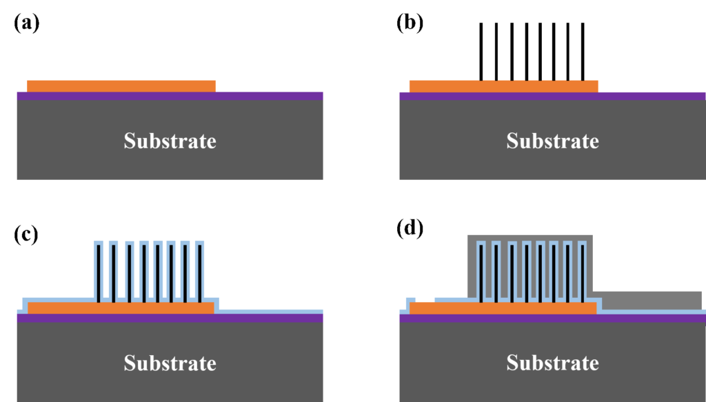
Silicon-based dielectrics are used within semiconductor manufacturing processes of high density electronic devices by semiconductor manufacturing processes. Silicon based dielectrics for capacitor technologies are usually based on silicon dioxide (MIS) or silicon nitride (MOS) insulating layers. Figure 1. below describes a conventional MOS technology to make silicon capacitors.
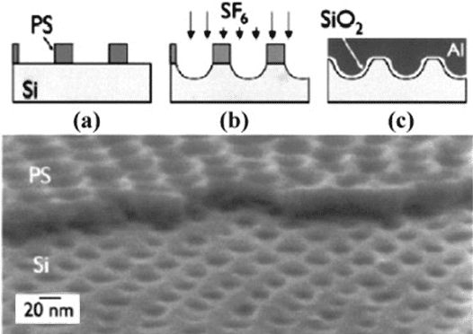
Conventional Technology MOS Capacitor Process
(a) Polymer template formation on silicon surface
(b) RIE pattern transfer of PS template into silicon, followed by the removal of the PS matrix.
(c) SiO2 growth followed by top Al gate electrode deposition
Silicon capacitors can be manufactured and used as
- fully MIS/MOS compatible back-end technology as part of passive integration platform
- hetero-integrated as Multiple-Chip-Module or flip-chip with other technologies (CMOS, MEMS, etc.) in a system in chip (SiP) or on chip (SoP)
- discrete chip SMD capacitors
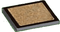
Single Layer RF Silicon Capacitors
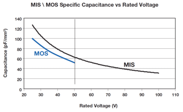
Silicon-based dielectrics are used to make low loss, high Q capacitors that feature very high temperature stability, high breakdown voltage and low leakage parameters. The main limitation is relatively low permittivity. Comparison of MIS and MOS dielectrics – see Table 1. and Figure 2. below.

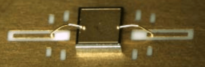
Gold or aluminum wire thermosonic and ultrasonic bonding are the most common way to assemble the single layer silicon capacitors (SLCs) in RF applications. Termination styles may differ and it can be optimized for epoxy or solder die attach mounting techniques. Examples – see Figure 3.

RF Thin Film Silicon Capacitors
Silicon thin film capacitors (Figure 4.) are typically based on a single layer silicon oxide/nitride dielectric deposited on a substrate and packed in a chip MLCC like design. It offers unique ability of very low capacitance values (0.05pF) and very tight capacitance tolerances (±0.01pF). Thin film technology guarantees minimal batch to batch variability of parameters at high frequency and thus it is an ideal component for RF and microwave filters.

Thin Film vs Silicon Capacitors – Practical Distinction
The term “thin film capacitors” covers a broader class of parts than those strictly fabricated on silicon substrates. Thin dielectric films can be deposited on alumina, quartz, silicon, or other substrates, and may use dielectric systems ranging from silicon oxides and nitrides to ceramic or organic films.
In practical design work, it is therefore useful to distinguish devices mainly by substrate and integration level. Thin film capacitors on alumina or quartz are typically delivered as discrete RF components in standard JEDEC packages and are optimized for very low capacitance values, tight tolerance and high Q at microwave frequencies. Silicon thin film capacitors and single-layer silicon capacitors (SLC) use silicon substrates and are often intended for integration by wire bonding, flip‑chip, or embedding techniques, where their thermal and mechanical compatibility with semiconductor processes is a key advantage.
Devices aimed at RF tuning and matching networks tend to be low‑capacitance, single‑layer structures with extremely tight tolerance and minimal batch‑to‑batch variability. By contrast, high‑density 3D silicon capacitors and wafer‑level CNF–MIM structures allow significantly higher specific capacitance and are optimized for broadband decoupling, DC blocking and power integrity functions, where larger tolerances are acceptable. Across this spectrum, both thin film and silicon capacitors are premium performance components and command substantially higher prices than commodity MLCCs with similar nominal capacitance and voltage ratings.
Thus, distinction between “thin film”(deposited on silicon substrate) and “silicon” capacitors is something of a marketing concession, though significant differences exist within & among the two depending on the intended application.
Devices targeting RF tuning & matching applications tend to be low-capacitance, single-layer devices optimized for parameter stability and consistency, and are commonly found in standard JEDEC package sizes.
In contrast, devices intended for power supply decoupling, broadband DC blocking, and similar applications allow larger tolerances in favor of achieving higher specific capacitance, and are more likely to be found in packaging adapted to advanced assembly methods such as wire bonding or embedding within a PCB. Regardless of intended application however, devices in the thin film and silicon capacitor families are premium-performance products and are priced accordingly, currently fetching something on the order of 5 to 5000 times the price of ceramic devices with similar capacitance and voltage ratings.
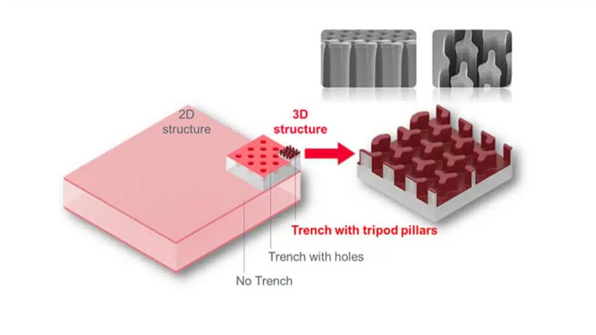
3D Silicon High Density Capacitors
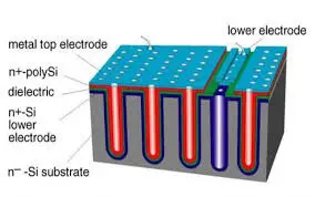
High density silicon capacitors are usually fabricated in ultra-deep trenches to increase surface area of electrodes. They have very low leakage current and low loss factor. Passive integration connective substrate (PICS) is the most common technology for implementing high density capacitors. This process allows implementation of multi-chip modules (MCMs) and chip on board (COB), and it helps to realize smaller components with low power consumption. In addition, this process allows integration of many basic functions into a single product, thereby helping to cut manufacturing costs. See Figure 5. on right – 3D PICS capacitor structure.
By employing latest 3D technologies, high volumetric efficiencies up to 1300nF/mm2 have been achieved. Silicon capacitors can be manufactured in layers below 100um that are 4xthinner than those of multilayer ceramic capacitor (MLCC) technology. Manufactured of silicon capacitors are claiming 10x better reliability in comparison to MLCC capacitors and in combination with ultra high temperature stability up to 250C, the high density silicon capacitor technology enable number of high demanding applications in automotive, industrial/oil drilling or aerospace/defense industry. It is expected that the volumetric efficiency of silicon capacitors will continue to improve as the demand for high performance and miniaturised components continues to grow.
Silicon capacitors – key features
- High Q, low losses, Low ESR and ESL over a broad frequency range, with usable performance extending into the GHz region depending on structure and package.
- Thin layers sub 100um possible
- High temperature operation (up to 250C), Wide voltage rating spectrum, typically from low‑voltage on‑chip decoupling up to tens of volts for discrete RF and high‑density devices, defined by process limits and dielectric system.
- High reliability lifetime expectancy (10x better than MLCC, as example: full rated 10V continuous operation at 250°C for 50years)
- Low leakage < 30nA/mF; Higher leakage current at high temperatures (but still 1000x lower compare to the other technologies)
- No/low radiation sensitivity
- No derating required
- No catastrophic failure mode
- Low weight
- Stable performance with tight capacitance tolerances, Tight capacitance tolerance options (down to ±0.01 pF for RF thin film devices, and typically ±5–10% for high‑density silicon capacitors).
- No piezo effect
- Non-magnetic
- Relatively low permittivity
Silicon Wafer Based Integrated Capacitors
Integrated capacitors and passives have a lot going for them. They take up less space on a PCB, they simplify design and they can, with the right processes shrink circuit tolerances thanks to closer component matching. The downside is that, as with semiconductors, volume is everything.
Although a common reason for keeping passive components off-chip is their size relative to that of the transistors on-die – is not worth wasting precious silicon area on devices that cost more to assemble than their materials are worth – many off-the-shelf parts rely on passives to tune filters and control loops for specific applications.
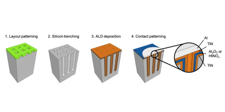
Utilization of semiconductor fabrication processes, however, has resulted in number of new approaches towards high density micro-capacitors. Finish company Picosun used its atomic layer deposition ALD equipment, to deposit film stacks of conductive TiN and insulating dielectric Al2O3 and HfAlO3 layers into high aspect ratio trenches etched into silicon that increased capacitance density up to 1 µF/mm2. ALD deposition and 3D microcapacitor manufacturing process is shown in Figure 6. below.
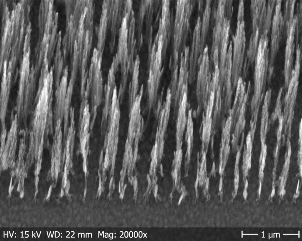
Swedish company Smoltek received Outstanding and Best Paper Award at EPCI PCNS conference for their carbon nano-fiber metal-insulator-metal (CNF-MIM) wafer based semiconductor technology achieving capacitance density to +650nF/mm2 at the end of 2019. They used ALD technique to deposit Al2O3/HfO2 layers onto carbon nano-fiber 3D structure.
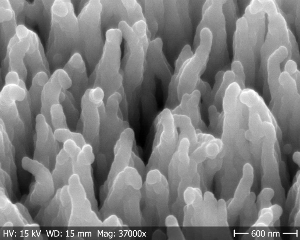
The fiber length is only 2 – 3 µm and the total height profile of the complete device is ca 4 µm. This makes the capacitors readily available for integration onto a CMOS chip or in 3D stacking. Figure 7-9. below shows the CNFs after the dielectric coating via ALD, the image showing a coating of Al2O3/HfO2/Al2O3 (5/3/5 nm). The dielectric layer is uniformly covering the individual CNFs.
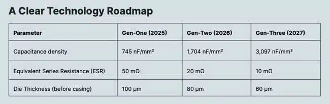
In update of Smoltek technology, the company released in 2025 its commercialization strategy document that includes the CNF-MIM capacitors technology roadmap as shown in Fig. 10.
Technology Roadmap and Future Directions
The evolution of silicon-based capacitors is strongly driven by the need for higher capacitance density, lower profiles and closer integration with semiconductor devices. Technologies such as ALD‑processed high‑k dielectrics in deep trenches and CNF–MIM wafer structures demonstrate that capacitance densities in the hundreds of nF/mm² to around 1 µF/mm² range are already achievable, with published roadmaps indicating further growth.
At present, adoption is most advanced in high‑value and high‑reliability markets, including automotive powertrain, aerospace and defence electronics, and high‑end processors and RF front‑ends, where the benefits in stability and reliability justify the higher cost. As manufacturing processes mature and integration with standard CMOS and packaging flows improves, silicon capacitors are likely to move further into mainstream power integrity and RF applications, particularly in systems‑in‑package and 3D‑stacked architectures.
Silicon Capacitors vs MLCC and Other Technologies
Silicon capacitors and multilayer ceramic capacitors (MLCCs) often compete for similar functions, but their characteristics and optimal use cases differ significantly. The following points highlight the most important contrasts for design engineers.
- Capacitance and volumetric efficiency
MLCCs offer very high absolute capacitance values in small SMD packages, but their effective capacitance can drop significantly under DC bias and over time. Advanced 3D silicon and wafer‑integrated capacitors can achieve very high specific capacitance per unit area (up to around 1 µF/mm² in reported trench‑based structures), but absolute capacitance in a single discrete device is still more limited than in MLCCs of similar footprint. - Temperature range and stability
Standard MLCC dielectrics such as X7R and X8R are typically specified up to 125–150 °C and show capacitance change with temperature and applied voltage. Silicon capacitors can be designed for continuous operation up to about 250 °C with excellent stability versus temperature and voltage, no DC bias derating and no capacitance ageing. - Reliability and failure mode
MLCCs are prone to mechanical cracking, piezoelectric effects and, in some cases, catastrophic short‑circuit failures under stress. Silicon capacitors exhibit very high failure‑in‑time (FIT) performance, no piezoelectric behaviour and no catastrophic failure mode, making them particularly attractive in high‑reliability and safety‑critical systems. - Frequency behaviour
MLCCs provide low impedance over a broad frequency range but suffer from resonance effects and ESL at very high frequencies. Silicon RF and thin film capacitors are optimized for high Q and stable parameters well into the GHz range, while high‑density silicon capacitors and CNF–MIM structures can offer low losses and predictable impedance profiles for broadband decoupling. - Cost and availability
MLCCs are commodity components with wide availability and low cost per capacitance unit. Silicon capacitors are premium devices, often produced in lower volumes and targeted at demanding applications, and therefore can cost from several to orders of magnitude more than MLCCs with similar nominal ratings.
For many designs, this leads to a hybrid solution where MLCCs provide bulk capacitance and cost‑effective decoupling, while silicon capacitors are reserved for positions requiring extreme stability, high temperature capability, or integration into semiconductor‑based structures
Frequently Asked Questions about Silicon Capacitors
Silicon-based capacitors use silicon dioxide or silicon nitride dielectrics, fabricated with semiconductor technology. They can be manufactured as metal-insulator-metal (MIM) structures and are used for high stability, reliability, and miniaturization applications.
Applications demanding high temperature stability and reliability—such as avionics, automotive systems, oil exploration, and military electronics—benefit most from silicon capacitors. Their stable capacitance at high temperatures makes them ideal for harsh environments.
– High stability at high temperatures (up to 250°C)
– Excellent leakage current stability
– High potential for miniaturization
– Low failure rates and long lifetimes
– No ageing under DC bias conditions
– Limited maximum achievable capacitance
– Increased charge leakage as the dielectric thickness decreases
– Relatively low permittivity compared to ceramic types
– Higher cost compared to MLCCs
Manufacturers use 3D nano-structured electrodes, ultra-deep trench fabrication, and atomic layer deposition (ALD) to increase surface area and volumetric efficiency, enabling thin layers and higher capacitance densities. Technologies from companies like Picosun and Smoltek use ALD for record capacitance density integration.
How to Select and Use Silicon Capacitors for High-Density, High-Reliability Applications
- Identify Application Requirements
Determine if your project demands high temperature stability, low leakage, miniaturization, or integration into semiconductor packages and advanced multi-chip modules.
- Choose the Appropriate Silicon Capacitor Structure
– For RF applications: Select single-layer or thin-film silicon capacitors with low capacitance, high Q, and stability.
– For high-density needs: Opt for 3D integrated capacitors with ultra-deep trench structures and higher volumetric efficiency. - Evaluate Performance Parameters
Review the temperature range (up to 250 °C), leakage current specifications, capacitance stability, tolerances, and expected lifetime. Check ESR and ESL versus frequency and compare them to alternative technologies such as MLCCs or thin film RF capacitors, especially if the capacitor serves a critical decoupling or matching function. For RF and microwave applications, verify Q‑factor and tolerance at the operating frequency, while for power and decoupling functions, focus on impedance profile over the relevant frequency band.
- Consider Fabrication and Mounting Options
Decide between discrete SMD types, embedded capacitors within PCBs, or integration with CMOS/MEMS as system-in-chip or system-on-package. Check compatibility with wire bonding and surface mount techniques.
- Assess Cost vs. Performance
Silicon capacitors are premium components with higher costs than MLCCs, but offer substantial reliability, miniaturization, and performance benefits in demanding environments.Designers should also be aware of a few typical pitfalls when adopting silicon capacitors. It is important not to assume MLCC‑like derating rules or failure modes: silicon capacitors do not exhibit DC bias capacitance loss or ageing, but their maximum capacitance and voltage ratings are strictly defined by the process and dielectric strength. Careful checking of mounting and process compatibility (wire bonding, embedding, reflow profiles) is required, especially when integrating high‑density wafer‑level or 3D structures into advanced assemblies.