Passive Components Blog
No Result
View All Result
  • Home
  • NewsFilter
    • All
    • Aerospace & Defence
    • Antenna
    • Applications
    • Automotive
    • Capacitors
    • Circuit Protection Devices
    • electro-mechanical news
    • Filters
    • Fuses
    • Inductors
    • Industrial
    • Integrated Passives
    • inter-connect news
    • Market & Supply Chain
    • Market Insights
    • Medical
    • Modelling and Simulation
    • New Materials & Supply
    • New Technologies
    • Non-linear Passives
    • Oscillators
    • Passive Sensors News
    • Resistors
    • RF & Microwave
    • Telecommunication
    • Weekly Digest

    YAGEO Releases Compact Coupled Inductors for High-Density VR Designs

    Enhancing Energy Density in Nanocomposite Dielectric Capacitors

    Advances in the Environmental Performance of Polymer Capacitors

    Vishay Releases DLA Tantalum Polymer Capacitors for Military and Aerospace

    Vishay Expanded Inductor Portfolio With More Than 2000 Stock Items 

    Paumanok Releases Capacitor Foils Market Report 2025-2030

    Modelithics Welcomes CapV as a Sponsoring MVP

    Wk 40 Electronics Supply Chain Digest

    Benefits of Tantalum Powder Stress–Strain Curve Evaluation vs Conventional Wet Test

    Trending Tags

    • Ripple Current
    • RF
    • Leakage Current
    • Tantalum vs Ceramic
    • Snubber
    • Low ESR
    • Feedthrough
    • Derating
    • Dielectric Constant
    • New Products
    • Market Reports
  • VideoFilter
    • All
    • Antenna videos
    • Capacitor videos
    • Circuit Protection Video
    • Filter videos
    • Fuse videos
    • Inductor videos
    • Inter-Connect Video
    • Non-linear passives videos
    • Oscillator videos
    • Passive sensors videos
    • Resistor videos

    Connector PCB Design Challenges

    Efficient Power Converters: Duty Cycle vs Conduction Losses

    Ripple Steering in Coupled Inductors: SEPIC Case

    SEPIC Converter with Coupled and Uncoupled Inductors

    Coupled Inductors in SEPIC versus Flyback Converters

    Non-Linear MLCC Class II Capacitor Measurements Challenges

    Percolation Phenomenon and Reliability of Molded Power Inductors in DC/DC converters

    Root Causes and Effects of DC Bias and AC in Ceramic Capacitors

    How to Calculate the Output Capacitor for a Switching Power Supply

    Trending Tags

    • Capacitors explained
    • Inductors explained
    • Resistors explained
    • Filters explained
    • Application Video Guidelines
    • EMC
    • New Products
    • Ripple Current
    • Simulation
    • Tantalum vs Ceramic
  • Knowledge Blog
  • Suppliers
    • Who is Who
  • Events
No Result
View All Result
Passive Components Blog
No Result
View All Result

Nano Dimension Demonstrated 3D Printed High Density Interconnect PCB

18.6.2021
Reading Time: 2 mins read
A A

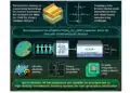
The ongoing technological revolution continues to introduce more and more innovative design and production methodologies for manufacturing highly- efficient electronic PCB products. One of this is High Density Interconnect (HDI) PCB by Additively Manufactured Electronics (AME) technology.

Being multi-layer, HDI boards have both buried and blind vias to provide more interconnections and signal integrity solutions. To achieve the desired stack up layers or sequential lamination cycles, conventional manufacturing processes require multiple drilling procedures that inevitably increase the time, complexity and cost of production.

RelatedPosts

YAGEO Releases Compact Coupled Inductors for High-Density VR Designs

Enhancing Energy Density in Nanocomposite Dielectric Capacitors

Advances in the Environmental Performance of Polymer Capacitors

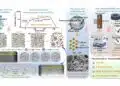
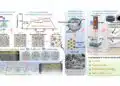
Nano Dimension AME technology combines all bonding, lamination, drilling and plating into one simultaneous, short and comprehensive high-quality printing procedure. In fact, the lead-time for printing an HDI PCB using AME technology is about the same as for producing a standard plated through hole PCB.

Process Complexity and Duration

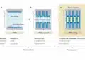
The conventional manufacturing of a plated through hole PCB is a multi-step process that requires lamination, drilling and plating. Manufacturing an HDI PCB requires laser drilling, plating and then adding top / bottom layers. This adds complexity and increases the duration of the process as the number of layers increases. An HDI PCB with 6 layers and stacked vias takes between 2 to 3 weeks to manufacture. With AME technology, printing a 60mm x 60mm x 1mm PCB board takes less than a day, regardless of the number of stacked vias and layers.With conventional PCB manufacturing, creating a stack via using a back drill increases the prepreg thickness, and therefore the overall PCB thickness. The thickness of the prepreg of an HDI PCB manufactured using AME can be any size above the minimum requirement.

This one-step process additively builds the HDI PCB layers including the conductive layers, prepreg, PTH, stacked vias, solder mask and solder pads.Any number of layers is applicable within the total board thickness requirements (3mm) considering the thickness of the conductive and prepreg layers.

Impedance Control

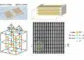
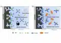
Using a laser drill and then plating stacked vias can cause disconnections. Filling laser drilled vias is complex and staggering vias generates impedance control challenges. During production, vias are stacked with offset. This results in problematic extensions and impedance imparity.

With AME technology manufacturing stacked blind / buried vias is simple, assuring impedance control without stubs or losses from via stubs.

Related

Source: Nano Dimension

Recent Posts

Enhancing Energy Density in Nanocomposite Dielectric Capacitors

9.10.2025
6
a Schematic diagram of the BNT-based components constructed based on the entropy-increase strategy. b Digital photograph, cross-sectional SEM image, and EDS mappings of the MLCCs. c Unipolar P-E loops of MLCCs as a function of applied E. d Wrec and η of the MLCCs as a function of applied E. The comparison of (e) Wrec and η, (f) η and UF of the MLCCs with those of other recently reported state-of-the-art MLCCs. source: Nature Communications

Researchers Proposed Enhanced Energy Storage MLCC

1.10.2025
19

Development of Nitrogen-Doped Graphene Supercapacitors 

30.9.2025
11

Researchers Developed Reduced Graphene Oxide (rGO) High Energy Density Graphene Supercapacitors

18.9.2025
35

Researchers Enhanced 2D Ferromagnets Performance

16.9.2025
9

Researchers Demonstrated HfO Anti-Ferroelectric Flexible Capacitors

19.8.2025
21

Additive Manufacturing of Mn-Zn Ferrite Planar Inductors

4.8.2025
44

Researchers Presents High-Performance Carbon-Based Supercapacitors

1.8.2025
44

Researchers Demonstrated 200C Polymer Film Dielectric

28.7.2025
24

Researchers Demonstrated Zinc-Ion Based Photo-Supercapacitor

28.7.2025
22

Upcoming Events

Oct 14
16:00 - 17:00 CEST

Smart Sensors, Smarter AI: Building Reliable Edge Systems

Oct 17
12:00 - 14:00 EDT

External Visual Inspection per MIL-STD-883 TM 2009

Oct 20
October 20 - October 23

Digital WE Days 2025 – Virtual Conference

Oct 21
October 21 @ 12:00 - October 23 @ 14:15 EDT

Space and Military Standards for Hybrids and RF Microwave Modules

Oct 28
8:00 - 15:00 CET

Power Up Your Design: SN6507 and the Ready-to-Use Development Kit

View Calendar

Popular Posts

  • Buck Converter Design and Calculation

    0 shares
    Share 0 Tweet 0
  • Boost Converter Design and Calculation

    0 shares
    Share 0 Tweet 0
  • Flyback Converter Design and Calculation

    0 shares
    Share 0 Tweet 0
  • LLC Resonant Converter Design and Calculation

    0 shares
    Share 0 Tweet 0
  • What is a Dielectric Constant and DF of Plastic Materials?

    4 shares
    Share 4 Tweet 0
  • SEPIC Converter Design and Calculation

    0 shares
    Share 0 Tweet 0
  • Dual Active Bridge (DAB) Topology Explained

    0 shares
    Share 0 Tweet 0
  • Ripple Current and its Effects on the Performance of Capacitors

    3 shares
    Share 3 Tweet 0
  • MLCC and Ceramic Capacitors

    0 shares
    Share 0 Tweet 0
  • Flying Capacitors Explained

    0 shares
    Share 0 Tweet 0

Newsletter Subscription


Passive Components Blog

© EPCI - Leading Passive Components Educational and Information Site

  • Home
  • Privacy Policy
  • EPCI Membership & Advertisement
  • About

No Result
View All Result
  • Home
  • Knowledge Blog
  • Premium Suppliers

© EPCI - Leading Passive Components Educational and Information Site

This website uses cookies. By continuing to use this website you are giving consent to cookies being used. Visit our Privacy and Cookie Policy.
Go to mobile version