


Over-voltages and current spikes must be avoided in many areas of electronics; numerous laws and regulations in the various destination countries specify product safety in explicit terms.
Key Takeaways
- Over-voltage protection is critical for modern electronics to prevent damage from surges and spikes.
- Effective designs use a combination of protection components like MOVs, TVS diodes, and GDTs across multiple stages.
- MOVs are ideal for high-energy applications, while TVS diodes provide precise clamping in low-voltage environments.
- Proper PCB layout and component selection is essential for optimal protection performance.
- Designers should use standards like IEC 61000 for guidance on implementing effective over-voltage protection.
Introduction: Why Protection Matters
Modern electronic systems must withstand electrostatic discharge (ESD), lightning‑induced surges, fast transients, and short‑circuits without unsafe behavior or permanent damage. Over‑voltage and over‑current protection reduce field‑failure rates, help products pass compliance testing, and lower maintenance and repair costs across consumer, industrial, telecom, and automotive markets.
From a standards perspective, protection design is closely linked to immunity tests such as IEC 61000‑4‑2 (ESD), IEC 61000‑4‑4 (EFT/burst), and IEC 61000‑4‑5 (surge), as well as sector‑specific rules like automotive ISO 7637 and LV 124 or safety standards for mains‑connected equipment. Understanding the transient environment and applicable tests is the first step in choosing appropriate protective components.
Static discharges and over‑voltages (transients) can destroy circuits. If a surge voltage that exceeds the permissible operating voltage of an IC is applied to a circuit, it can permanently damage the IC.
To clamp these damaging transients – that is, to deflect them to ground potential and protect the IC – different components for over‑voltage protection are available. These include metal oxide varistors (MOV), transient voltage suppressor (TVS) diodes, gas discharge tubes (GDT) and ESD protection diodes.
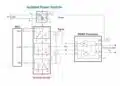
System‑Level Protection Concept
Figure 1 provides a schematic overview of the various types and levels of protective elements for electronic circuits. In practice, robust designs almost always use multiple stages of protection coordinated along the energy path from the outside world into sensitive IC pins.
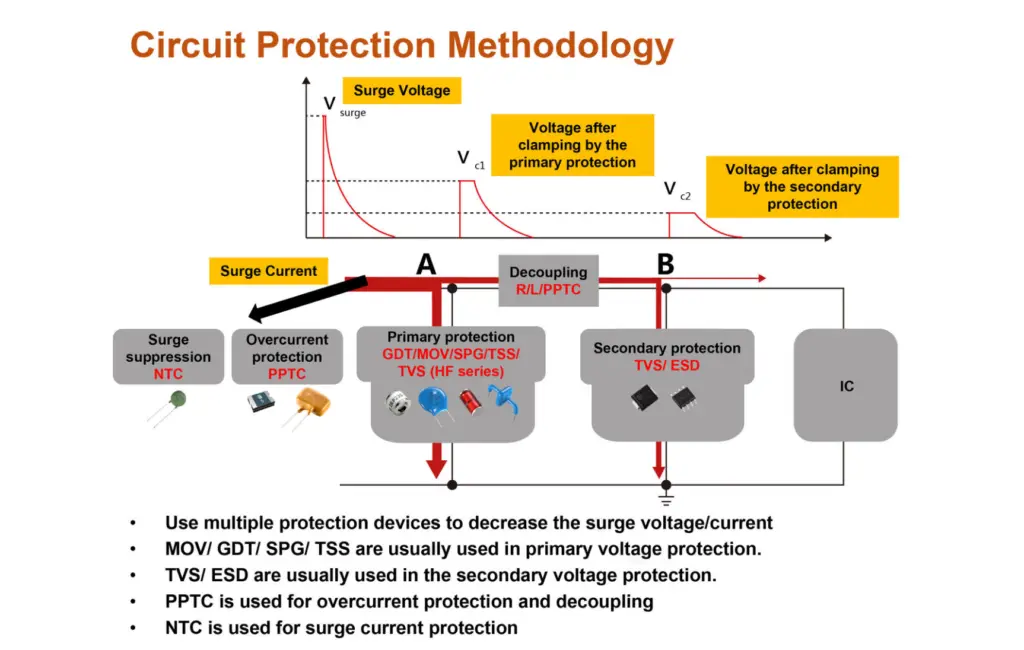
Components such as MOV, GDT, spark gap protectors (SPG) and thyristor surge suppressors (TSS) serve as primary protection against large over‑voltages at the interface to the outside environment. TVS and ESD components provide secondary protection closer to the IC, while polymeric PTC (PPTC) and NTC thermistors, fuses and current‑sense resistors address over‑current and inrush events.
PPTCs act as over‑current protection and as decouplers, while NTCs are used to suppress inrush currents or shape start‑up behavior. Good PCB layout keeps these protection elements physically close to connectors and defines short, low‑inductance paths to the return plane (ground) to minimize residual stresses on protected circuits.
Varistors: Fast, High‑Energy Surge Protection
Varistors score highly thanks to their short response time
Due to their very short response time, varistors are used in numerous applications for clamping transient over‑voltages in the sub‑20‑ns range. The best known are metal oxide varistors (MOV), which are capable of absorbing high‑energy over‑voltages and significantly higher surge currents than TVS diodes of comparable size.
MOVs are manufactured primarily from zinc oxide and cover a wide voltage range from around 18 to 1800 V with surge currents up to tens of kiloamperes for standardized lightning surge waveforms. Typical datasheets specify maximum current Ipp for an 8/20 µs pulse, operating temperature ranges up to 105 °C or 125 °C, and a bidirectional, symmetric breakdown characteristic.
Such MOVs are widely used in AC mains inputs, signal lines in industrial control systems, LED drivers, smart metering systems and over‑voltage categories defined in safety standards. Disc diameters from a few millimeters up to 50 mm and different lead/terminal options allow tailoring of surge capability to the application.
Combination devices that integrate an MOV with an in‑series NTC or thermal element can provide coordinated limitation of both surge voltage and follow‑on current, especially in mains connected equipment. These assemblies can simplify safety approvals and reduce component count in compact power supplies.
The main disadvantage of MOVs is aging: each absorbed surge slightly degrades the device and shifts its characteristics, leading to a finite service life that depends on the number and magnitude of surges. For higher robustness, designers often use MOVs in series with GDTs or SPGs so that only residual energy reaches the MOV in severe surge events.
TVS Diodes: Precise, Low‑Capacitance Clamping
TVS diodes guarantee rapid unidirectional or bidirectional blocking
TVS diodes (also called suppressor diodes, avalanche breakdown diodes or transient voltage protectors) clamp over‑voltage peaks within picoseconds to nanoseconds and confine them to safe levels for the protected circuit. They are connected in parallel to the load and act as a rapid shunt path for transient current once their breakdown voltage is exceeded.
The primary advantages of TVS diodes are their very short response time, low series resistance and low capacitance versions for high‑speed interfaces. Devices are available in unidirectional and bidirectional variants for DC supplies, communication lines, automotive loads and signal interfaces.
TVS portfolios typically span peak pulse powers from a few hundred watts up to tens of kilowatts for standardized 10/1000 µs pulses and a wide range of reverse standoff voltages, for example from 3.3 V up to 600 V and beyond. Standard packages include SMA/SMB/SMC and axial DO‑style through‑hole packages, with automotive‑qualified parts available for many ratings.

MOV vs. TVS: When to Choose Which?
Figure 3 shows a qualitative comparison of MOV and TVS characteristics. The table below summarizes typical trade‑offs for mains and low‑voltage applications.

Table 1 – Typical characteristics of MOV vs. TVS
| Feature | MOV (Varistor) | TVS Diode |
|---|---|---|
| Response time | Fast (ns), but slower than TVS | Very fast (ps–ns range) |
| Energy handling | Very high surge energy, kA range | Lower energy per device |
| Voltage range | Wide (tens to thousands of volts) | Low to medium (few volts to hundreds) |
| Clamping accuracy | Coarse, higher residual voltage | Tight clamping window |
| Capacitance | High to very high | Low, very low types for high‑speed lines |
| Aging / wear‑out | Yes, cumulative with surge stress | Much less aging under normal use |
| Typical use | AC mains, power distribution, high‑energy surges | DC rails, data lines, automotive I/O |
As a rule of thumb, MOVs are preferred for high‑energy, higher‑voltage environments such as AC mains and industrial lines, while TVS diodes are the component of choice for precise clamping on low‑voltage supply and signal rails.
Other Protection Components
TVS arrays are multi‑channel TVS solutions tailored for ESD and surge protection of high‑speed interfaces such as HDMI and USB. They are offered for operating voltages matched to IC supply rails (for example 2.8 to 36 V) and with total capacitance frequently below 1 pF per line.
Spark gap protectors (SPG) provide high‑voltage isolation and spark‑over at defined voltages between roughly 140 and 5000 V with surge ratings in the 300 to 3000 A range for typical surge waveforms. They offer high insulation resistance in normal operation and can be used in coordination with MOVs or GDTs to handle extreme surges.
Gas discharge tubes (GDT) are sealed gas‑filled devices with very high isolation resistance (around giga‑ohms) and high surge capability from hundreds of amperes up to 100 kA for standardized pulses. Typical DC spark‑over voltages range from 75 to 6000 V with somewhat higher impulse spark‑over values, making them suitable for coaxial, telecom and Ethernet line protection.
Thyristor surge suppressors (TSS) are crowbar‑type devices used mainly in telecom and metering applications, combining relatively low leakage current with precise turn‑on at defined breakover voltages. Typical peak currents are in the hundreds of amperes for 8/20 µs pulses and they are often combined with series resistors or PPTCs.
PPTC resettable fuses act as over‑current protectors: under normal conditions they exhibit low resistance, but when the current exceeds the hold current Ihold for a sufficient time, self‑heating drives them into a high‑resistance state. Typical Ihold ratings span tens of milliamperes to double‑digit ampere ranges with maximum voltage ratings up to several hundred volts.
NTC thermistors with stable cycling behavior are widely used for inrush current limiting in power supplies, UPS systems and adapters. Disc sizes from 5 mm to 25 mm allow tailoring of the resistance and energy handling to the input power level.
Design Examples
Example 1: Mains Input Protection for an SMPS
For a 230 VAC off‑line power supply, a common protection structure includes:
- Primary surge stage at the AC inlet, for example a GDT or SPG plus a suitably rated MOV between line and neutral.
- Inrush current limiter, typically an NTC in series with the line, dimensioned for expected cold‑start energy and steady‑state dissipation.
- Over‑current protection using a fuse or PPTC device in series with the line, suitable for safety approvals and fault conditions.
- Secondary protection, e.g. a TVS diode across the DC bus or directly at sensitive controller supply rails.
The MOV’s working voltage is selected above the peak of the highest expected mains voltage but low enough to clamp surge levels below the withstand voltage of downstream components. Energy ratings and derating must consider both standardized surge tests (such as IEC 61000‑4‑5) and expected real‑world surges over the equipment’s lifetime.
Example 2: Automotive Sensor Input with Load Dump and ESD
For a 12 V automotive sensor input facing ISO 7637 pulses and ESD, a typical structure may include:
- A series resistor or inductor to limit surge current into the ECU input.
- A bidirectional TVS diode to clamp load‑dump transients and ESD events to a safe range.
- Optional RC filtering to improve EMC and reduce dV/dt at the IC input.
Here the TVS standoff voltage is chosen above the normal operating range of the line but below the maximum rating of the input circuitry when combined with the series impedance. Automotive‑grade (AEC‑Q101) TVS devices are recommended due to the harsh electrical environment.
Practical Selection Guidelines
Interpreting Selection Diagrams
In summary, a selection decision guideline for protective components can be visualized as in figure 4. The first branch typically distinguishes whether the primary concern is over‑voltage, over‑current, or both, and whether the interface is power, low‑speed signal, or high‑speed data.

For over‑voltage on power lines, designers normally start with the highest expected surge energy and voltage and then choose an appropriate combination of GDT/SPG and VAR or TVS, adding secondary TVS or ESD protection close to ICs. For ESD‑dominated high‑speed interfaces, low‑capacitance TVS arrays with suitable working voltage and line configuration are preferred.
Figure 5 provides examples of how different protection components match to typical applications such as AC line interfaces, telecom ports, sensor inputs and data buses. Designers often combine these diagrams with system specifications and mandatory test standards to arrive at a robust yet cost‑effective solution.

PCB Layout and Implementation Tips
Even with well‑chosen components, poor layout can compromise protection effectiveness. Key implementation guidelines include placing primary surge elements close to the entry point of the line or connector and keeping their connection to the reference plane as short and wide as possible.
Secondary TVS or ESD diodes should sit directly adjacent to the protected IC pins, with minimal trace inductance between the pin and the protection device. For mains and high‑voltage lines, creepage and clearance distances around MOVs, GDTs and spark gaps must respect the applicable safety standards and pollution degrees.
Summary of Component Roles
Table 2 – Typical roles of protection components
| Component | Main function | Typical interface |
|---|---|---|
| MOV | High‑energy surge clamping | AC mains, industrial power |
| TVS | Fast, precise voltage clamp | DC rails, low‑voltage I/O |
| GDT/SPG | Very high surge handling | Telecom, coax, primary surge |
| TSS | Crowbar for telecom lines | Telephone, metering, DSL lines |
| TVS array | ESD/surge on multi‑line ports | HDMI, USB, high‑speed data |
| PPTC | Resettable over‑current limit | I/O ports, low‑voltage power |
| NTC | Inrush current limiting | AC/DC power supplies, chargers |
How to Design a Basic Over-Voltage and Over-Current Protection Scheme
- Step 1: Define the electrical environment and standards
Identify the nominal operating voltage, maximum expected line variations and types of disturbances the circuit must survive, such as ESD, lightning-induced surges or automotive pulses. Map these conditions to relevant standards like IEC 61000-4-2, IEC 61000-4-4 and IEC 61000-4-5, or automotive ISO 7637 and LV 124, to understand required test levels and waveforms.
- Step 2: Classify the interface type
Determine whether the interface is an AC mains input, a DC power rail, a low-speed signal, or a high-speed data line. For mains and industrial power lines, focus on high-energy surge capability, while for data lines you must prioritize low capacitance and minimal impact on signal integrity.
- Step 3: Select primary surge protection components
Choose primary protection elements located at the point of entry, such as MOVs, GDTs or spark gap protectors. Select their working voltage above the highest normal operating voltage but low enough to keep clamped surge levels within the insulation and component ratings. Verify that their surge current and energy ratings exceed the worst-case surge levels with appropriate derating.
- Step 4: Add secondary clamping for sensitive circuits
For sensitive ICs, add secondary protection such as TVS diodes or low-capacitance TVS arrays close to the device pins. Match the TVS standoff voltage to the supply or signal level, and ensure the clamping voltage plus any series resistance stays below the absolute maximum ratings of the protected IC pins during surge and ESD events.
- Step 5: Implement over-current and inrush protection
Choose over-current protection components appropriate to the interface, such as fuses or PPTC resettable fuses for power rails and I/O lines. For power supplies with large input capacitance, use NTC inrush current limiters or controlled start-up circuits to reduce initial current spikes and stress on rectifiers, capacitors and protection components.
- Step 6: Optimize PCB layout for protection paths
Place primary surge components near connectors or entry points with short, wide traces to the reference plane to minimize inductance in the surge current path. Position secondary TVS or ESD components adjacent to the protected IC pins and ensure adequate creepage and clearance distances for mains and high-voltage nodes according to the applicable safety standards.
- Step 7: Validate performance with testing and iteration
Test the assembled design against the relevant ESD, surge and burst standards to confirm that protection devices trigger correctly and that no unsafe conditions or permanent damage occur. Use test feedback to adjust component ratings, combinations or PCB layout until the design provides reliable, repeatable protection over the expected lifetime of the product.
Conclusion
Over‑voltage and over‑current protection is a system‑level discipline that combines knowledge of the electrical environment, compliance standards and component behavior. By coordinating primary surge elements such as MOVs, GDTs or SPGs with secondary TVS and ESD devices and appropriate over‑current protection, designers can significantly improve the robustness and safety of their products.
Practical success depends not only on the choice of component type but also on correct voltage and energy ratings, proper derating and careful PCB layout at the interface to the outside world. Using structured selection guidelines, validated reference designs and real‑world test data helps ensure that protection circuits perform as intended over the full product lifetime.
FAQ about Over-Voltage and Over-Current Protection
Over-voltage protection prevents electronic circuits from being damaged by voltage spikes such as ESD, lightning-induced surges and fast transients. It uses dedicated components like MOVs, TVS diodes and gas discharge tubes to clamp dangerous voltages to safe levels for ICs and other sensitive devices.
Over-current protection limits excessive current that can overheat conductors, damage components or create safety risks. Designers commonly use fuses, PPTC resettable fuses, NTCs and current-sense resistors to detect and limit fault currents or inrush currents in power supplies and interfaces.
Typical over-voltage protection components include metal oxide varistors (MOV), transient voltage suppressor (TVS) diodes, gas discharge tubes (GDT), spark gap protectors (SPG), thyristor surge suppressors (TSS) and TVS arrays. Each component type targets specific surge levels, voltage ranges and interface types.
MOVs are preferred in high-energy, higher-voltage environments such as AC mains and industrial power lines where large surge currents must be absorbed. TVS diodes are better suited to low-voltage rails and data lines where precise clamping, low capacitance and very fast response are required.
TVS arrays integrate multiple low-capacitance TVS diodes in one package to protect differential and multi-line interfaces such as HDMI, USB and Ethernet. They provide fast ESD and surge clamping while keeping line capacitance low enough to preserve signal integrity at high data rates.
Gas discharge tubes and spark gap protectors act as primary surge arresters, offering very high insulation resistance during normal operation and very high surge current capability when a surge exceeds their spark-over voltage. They are often used on telecom, coaxial and mains interfaces, sometimes in combination with MOVs and TVS diodes.
PPTC devices operate with a low resistance in normal conditions. When current exceeds their hold current for a sufficient time, internal heating increases their resistance dramatically and limits the current. After the fault is removed and the device cools, it returns close to its original low-resistance state.
NTC inrush limiters start with a relatively high resistance when cold, which limits the initial surge current when a power supply is switched on. As current flows, the thermistor heats up and its resistance drops, allowing efficient normal operation with low power loss.
Designers should consider EMC immunity standards such as IEC 61000-4-2 for ESD, IEC 61000-4-4 for EFT/burst and IEC 61000-4-5 for surge tests. In automotive applications, standards like ISO 7637 and LV 124 define the pulse environment and test conditions for electrical disturbances in road vehicles.
PCB layout is critical: protection components should be placed close to connectors and IC pins, with short, wide traces to ground to minimize parasitic inductance. Adequate creepage and clearance distances are essential on mains and high-voltage sections to meet safety standards and avoid flashover during surge events.
References
- “A well‑equipped protection force – overvoltage and overcurrent protection components”, Rutronik and Yageo.
- IEC 61000‑4‑2/4‑4/4‑5 immunity test standards for ESD, EFT and surge (general reference).
- Automotive ISO 7637 and LV 124 standards for electrical disturbance in road vehicles (general reference).