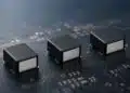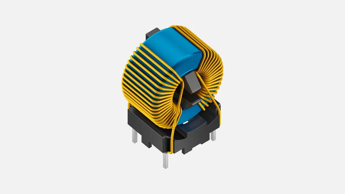
TDK has introduced the B82722V6*B040 series of high‑voltage, current‑compensated ring‑core double chokes for DC bus voltages up to 1250 V (630 V AC) in compact power electronics.
The high-voltage common mode choke components are aimed at power converters, industrial motor drives, and switch‑mode power supplies that increasingly use SiC and GaN power semiconductors and operate with elevated DC bus voltages, where EMI suppression, insulation coordination and PCB space are all critical design constraints.
Key features and benefits
The series is designed to combine very high voltage capability with a small vertical footprint, making it easier to realize high‑voltage architectures without enlarging the filter area.
- Voltage and insulation
- Designed primarily for DC voltages up to 1250 V and 630 V AC at 50/60 Hz.
- Uses multilayer solid insulation and is tested at 3,750 V line‑to‑line for robust electrical isolation in high‑voltage systems.
- Compact mechanical design
- Each choke measures about 23 × 15.5 × 24 mm (L × W × H) in a vertical through‑hole package.
- The ring‑core double choke structure and plastic header provide mechanical stability while keeping the PCB footprint small.
- Electrical range
- Nominal inductance options from 3.3 mH to 22 mH with a tolerance of −30/+50%.
- Rated currents from 0.85 A to 3.0 A at +70 °C, allowing a trade‑off between attenuation and current capability.
- EMI performance
- A special automated winding technique yields high resonance frequency characteristics, which is important for converters with fast edges from SiC/GaN switches.
- Typical stray inductance is about 0.6% of nominal inductance, giving some symmetrical‑mode (differential‑mode) impedance while keeping the main function focused on common‑mode suppression.
- Safety and compliance
- Epoxy‑coated ferrite core and UL 94 V‑0 compliant plastic header support fire safety and robustness.
- The design fulfills IEC 60938‑2 and IEC/UL 60939‑3 requirements for EMI chokes and filters and is RoHS‑compatible.
- Components are suitable for wave soldering, fitting standard THT production lines.
For design engineers, the net effect is a ready‑to‑use high‑voltage common‑mode choke that is small enough for dense layouts but still specified with clear insulation and test levels. For purchasers, the unified form factor across multiple electrical variants simplifies stocking and second‑sourcing within the same series.
Typical applications
TDK explicitly lists suppression of common‑mode interference, compact switch‑mode applications, and frequency converters as the primary applications for the B82722V6*B040 series. In practice, this translates into several concrete use cases.
In high‑voltage DC/DC and AC/DC converters, especially those with intermediate DC links around 800–1250 V, these chokes can be placed in the DC bus lines as part of the input or output EMI filter. They help to reduce common‑mode noise returning to the mains or coupling into sensitive control circuitry, which is particularly important when SiC or GaN power stages generate steep dv/dt transitions.
In industrial motor drives and frequency converters, the chokes may be used on the inverter side or near the DC‑link to limit common‑mode currents that would otherwise cause unwanted emissions, leakage currents, or additional stress on motor insulation and cable systems. The compact vertical format is advantageous in crowded drive cabinets where board area is scarce but a few extra millimeters of height are acceptable.
In compact SMPS for industrial, telecom, or server power, the combination of high bus voltage capability, small footprint, and high‑frequency behavior allows the chokes to serve as the core common‑mode element in a multi‑stage EMI filter, alongside X capacitors, Y capacitors, and optional differential‑mode chokes.
Technical highlights
The table below summarizes the key electrical data for the six members of the B82722V6*B040 family.
| Ordering code | Rated current at +70 °C (A) | Nominal inductance (mH, −30/+50%) | Stray inductance typ. (µH) | DC resistance typ. (mΩ) |
|---|---|---|---|---|
| B82722V6851B040 | 0.85 | 22 | 130 | 550 |
| B82722V6112B040 | 1.1 | 15 | 92 | 320 |
| B82722V6152B040 | 1.5 | 10 | 61 | 188 |
| B82722V6202B040 | 2.0 | 6.8 | 40 | 115 |
| B82722V6252B040 | 2.5 | 4.7 | 28 | 76 |
| B82722V6302B040 | 3.0 | 3.3 | 20 | 53 |
As current capability increases from 0.85 A to 3.0 A, the nominal inductance decreases from 22 mH to 3.3 mH, along with a reduction in DC resistance. This is the typical trade‑off in current‑compensated chokes: higher current devices offer lower impedance but lower losses and higher thermal margin; lower current devices offer higher impedance but must carry less current. The stray inductance values again confirm the roughly 0.6% ratio to the nominal inductance across the series.
Mechanically, all variants share the same vertical, epoxy‑coated toroidal core with plastic header, which simplifies PCB design because one footprint supports all six electrical options. The chokes are intended for wave soldering, which is still common in power electronics assemblies that use large capacitors, transformers, and other through‑hole components.
Design‑in notes for engineers
For practical design‑in, it is often helpful to think in terms of filter performance, thermal limits, and layout and safety. The points below summarize key aspects for each of these areas.
- Choosing the right variant
- Start from the required common‑mode impedance at the dominant interference frequencies, then select an inductance value that provides sufficient margin even at the −30% tolerance limit.
- Match the rated current at +70 °C with the worst‑case RMS current in your lines, including expected overloads and ambient temperature conditions.
- Use higher inductance / lower current parts when attenuation is critical and currents are modest; use lower inductance / higher current types where conduction losses and temperature rise dominate.
- EMI behavior and interaction with the rest of the filter
- The high resonance frequency of the winding structure is advantageous in SiC/GaN‑based converters with significant high‑frequency content, but it also means that interaction with Y capacitors, X capacitors and snubbers should be checked to avoid unwanted resonances.
- The approx. 0.6% stray inductance adds a small but non‑zero differential‑mode component; in simple filters this is often beneficial, but in tight designs it should be included in simulations or calculations.
- Thermal and mechanical considerations
- Confirm that copper losses (I²R) and any additional losses from high‑frequency currents remain within acceptable limits across the entire operating temperature range.
- Ensure enough vertical clearance and consider mechanical fixation if the system is subject to vibration, even though the epoxy‑coated core and plastic header already provide robust construction.
- Layout, safety, and standards
- Place the choke close to the noise entry/exit point (e.g. near connectors or DC‑link nodes) and route the two lines as a tight pair before and after the core to minimize loop area.
- Keep sensitive signal traces away from the choke to avoid unwanted coupling.
- Validate creepage and clearance distances around the pins and between isolated domains according to the relevant equipment standard, using the 3,750 V line‑to‑line test level and the IEC 60938‑2 / IEC/UL 60939‑3 classifications as input from the component side.
Overall, the B82722V6*B040 series offers a straightforward way to implement high‑voltage common‑mode filtering in compact power converters, especially where SiC and GaN switches demand more robust EMI control without sacrificing board space.
Source
This article is based on the official TDK Electronics press release for the B82722V6*B040 high‑voltage common‑mode choke series and the associated technical information provided on the TDK Electronics website, with additional independent commentary aimed at supporting design‑in and component selection for high‑voltage converter and drive applications.