


The voltage coefficient of resistance (VCR) is a key non‑linearity parameter of high‑value resistors that can quietly dominate error budgets in precision and high‑voltage circuits. While often ignored in low‑ohmic designs, VCR becomes critical once resistance values move into the tens of megaohms and beyond or when linearity over a wide voltage swing is required.
Key Takeaways
- The Voltage Coefficient of Resistance (VCR) characterizes resistance change relative to applied voltage, becoming critical in high-value resistors.
- VCR significantly affects precision in high-voltage circuits, especially beyond 10 MΩ due to non-linear behavior.
- Manufacturers often use MIL‑STD‑202 for standardized VCR testing, yet practical measurement can face challenges like environmental noise.
- Designers should incorporate VCR into their error budgets, particularly for applications involving high-impedance circuits and large voltage swings.
- Measuring VCR accurately requires careful setup to mitigate issues like self-heating, instrument accuracy, and environmental conditions.
This article explains what VCR is, how different resistor technologies behave, how to measure and specify it correctly, and how to design circuits that remain linear despite VCR.
1. Definition and Basic Theory
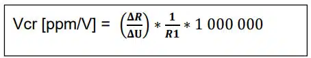
Analogous to the temperature coefficient of resistance (TCR), which describes resistance change versus temperature, VCR characterizes the change of resistance versus applied voltage. For a resistor whose resistance depends on the applied voltage , the VCR between two voltages and is defined as:where and are the resistance values measured at and , respectively.
The voltage coefficient of resistance (=Vcr), which is barely encountered at resistance values below 10MOhm, is a non-linear feature of resistors mainly at very high values.
Analog to the Tcr, which indicates the change of resistance with temperature, the Vcr reveals the change of resistance with applied voltage.
These resistors are non-ohmic resistors which means that the ratio between applied voltage and measured current is no longer constant for every voltage. So strictly speaking, if you use the well-known formula:
R = U / I
you have to specify the voltage at which you measure the resistance (which is not necessary for true ohmic resistors). The calculation of the Vcr is completely analogous to the calculation of the Tcr, you just have to replace the temperatures with the voltages:
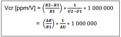
R1 = resistance value at voltage U1
R2 = resistance value at voltage U2
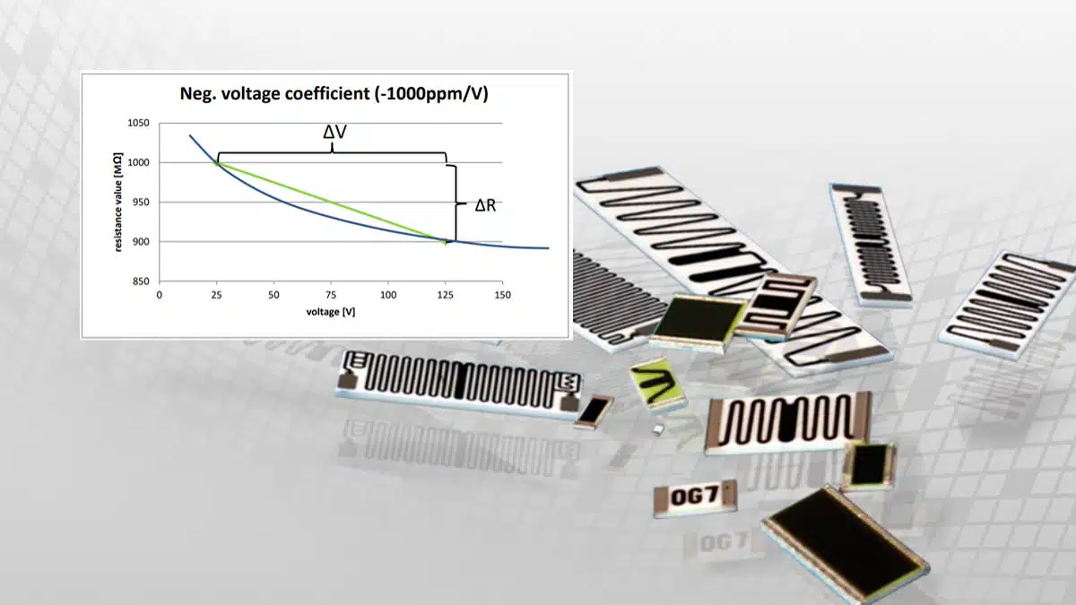
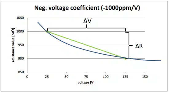
Exactly speaking (and this is valid for the Tcr too) this calculus is just the linear interpolation between the two measurement points at U1 and U2 (green straight line in the graph below). The real behaviour is nonlinear and could look like the one which is shown with the blue curve in the graph or similar.
If you rearrange the formula from above a little bit, you see that the Vcr is nothing else but the gradient or slope of R with V normalised to R1. It is easy to see in the graph on Figure 1. below, that the Vcr between 25V and 50V may be considerably different to the Vcr between 100V and 125V, albeit the voltage difference is in both cases ΔU = 25V.
Also, you see that when measuring the Vcr the exact value of the slope is important, and this is achieved by a big distance between the measurement voltages. Then small measurement errors of the resistance do not have such an influence.
Usually, the voltage coefficient is indicated in parts per million per volts [ppm/V] or also in percent per volt [%/V]; thick film resistors with ruthenium-oxide based conducting phase have negative Vcr’s. One example to see it more clearly:
A resistor with e.g. 1GOhm resistance value supposed to have a Vcr of lets say -1000ppm/V. Then the value of resistance will change from 1GOhm to 0,9GOhm (=-10%), if you change the voltage from 25V to 125V (voltage difference of ΔU = 100V). Analog this holds true for the Tcr.
Key points:
- VCR is usually expressed in ppm/V or %/V.
- Thick‑film resistors with ruthenium‑oxide conducting phase typically exhibit negative VCR (resistance decreases with increasing voltage).
- The calculation is a linear interpolation between two measurement points; the true curve is usually non‑linear.
Example: A 1 GΩ resistor with VCR = −1000 ppm/V will change from 1 GΩ at 25 V to about 0.9 GΩ at 125 V (−10%) for a 100 V increase.
2. Standardized VCR Specification (MIL‑STD‑202 Method 309)
Different manufacturers use different test conditions, which complicates comparison between parts. MIL‑STD‑202G, Method 309, defines VCR as:
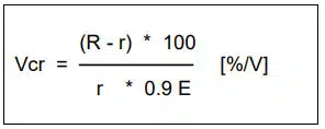
- R = resistance at maximum specified working voltage E
- E = maximum specified working voltage
- r = resistance at 10% of the maximum specified working voltage E
This means the voltage ratio is 10 and the absolute difference is 0.9·. However, this method is not widely applied in practice for two main reasons:
- Many resistors are rated up to 10 kV–100 kV or more, which demands specialized high‑voltage sources and fixtures.
- To avoid self‑heating of small SMD components, the standard calls for pulsed measurement, which increases complexity and is sensitive to RC time constants at very high resistances.
For these reasons, many manufacturers adopt a modified approach (lower voltages, continuous measurement) while preserving a sufficient voltage span for good slope accuracy.
3. VCR by Resistor Technology and Resistance Range
Although detailed numeric ranges are often proprietary or scattered across datasheets, some qualitative trends are well established. The table below summarizes typical behaviour:
Typical VCR Behaviour by Technology (Qualitative)
| Technology type | Typical resistance range where VCR matters | VCR sign & magnitude (qualitative) | Notes |
|---|---|---|---|
| Thick‑film (RuO₂) SMD | >10 MΩ, especially >100 MΩ | Negative, tens to thousands ppm/V | Strongly dependent on paste, firing profile, and geometry. |
| High‑voltage thick‑film | 10 MΩ–GΩ | Negative, optimized to low values | Long meander patterns and tailored pastes improve VCR. |
| Thin‑film (NiCr, TaN) | Up to a few MΩ | Very low, often negligible | VCR usually not specified; linear I-V behaviour dominates. |
| Bulk metal foil | Up to a few 100 kΩ | Extremely low | Used where ultra‑linearity is required; mainly low‑ to mid‑ohmic. |
| Wirewound | Low to mid values | Very low, unless inductive effects | VCR rarely a concern compared with parasitic inductance. |
| Carbon composition | Mid to high values | Larger non‑linearities possible | Often older technology; non‑linearity can be significant. |
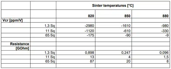
For thick‑film high‑ohmic parts, the paste formulation, sintering temperature, and layout geometry dominate VCR behaviour.
4. Influence of Paste, Sintering, and Geometry
For thick‑film resistors, both the conductive phase and the microstructure formed during firing determine the electric field distribution in the resistor. Industrial practice shows:
- VCR strongly depends on the resistive paste material.
- Sintering temperature can shift VCR dramatically; there is often an optimum firing window that minimizes VCR without compromising stability.
- Increasing the effective length‑to‑width ratio (L/B, “number of squares”) by using meander patterns usually improves VCR.
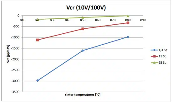
Manufacturers internal incoming inspection as an illustrative example: several component sizes with different L/B ratios are fired at different temperatures; VCR is then measured between 10 V and 100 V to identify the optimal process window. Figure 2 shows exactly such VCR vs. sintering temperature behaviour for a single paste.
5. Measurement of Low VCR – Practical Challenges
Measuring VCR at high resistance values is considerably more demanding than measuring TCR. Several pitfalls must be addressed to obtain meaningful data.
5.1 Key Measurement Issues
- Number of steady digits
At very high resistances (e.g., 100 GΩ), currents are in the picoampere range, and digit hopping makes it difficult to secure enough valid digits. To resolve differences such as 10 ppm/V vs. 20 ppm/V, you may need four or five stable digits, which is challenging in industrial environments at low voltages. - Measurement environment
Air humidity, airflows (HVAC, doors), and mechanical vibrations all introduce noise and drift in the setup, limiting the reliability of the last significant digit. Shielding, guarding, and environmental control are essential. - Measurement range changes
When measuring between 1 V and 10 V, the current changes by nearly a factor of ten. DMMs or electrometers often change measurement range, and each range has different accuracy, linearity, and offset, which can distort the calculated VCR. - Self‑heating and TCR interaction
At small packages, high voltage, and low VCR, self‑heating can cause resistance changes via TCR that are misinterpreted as VCR. External temperature changes also affect readings. - Instrument accuracy and limits
Above about 1 GΩ, current measurement accuracy of electrometers at 10 pA–100 pA is commonly around 0.5–1% of reading. One percent corresponds to 10,000 ppm; even across 100 V, this leaves ~100 ppm uncertainty in each measurement point. Statements like “1 ppm/V at hundreds of megaohms” should therefore be treated critically. - Measurement time and RC time constant
Large high‑value resistors have significant intrinsic capacitance ; cables and fixtures contribute external capacitance . The time constant is , and you should wait at least 5· to reach the final value, which can take many minutes.
5.2 Practical Measurement Recommendations
- Use guarded, shielded fixtures and high‑insulation materials.
- Avoid auto‑range changes between and ; fix ranges if possible.
- Allow sufficient settling time after each voltage step (multiple time constants).
- Verify consistency by repeating measurements and, when feasible, validating with a second instrument.
6. Circuit‑Level Impact and Error Budgeting
VCR directly translates into voltage‑dependent gain or scale error in circuits where the resistor carries a significant voltage. The most obvious examples are:
- Transimpedance amplifiers (TIA) with high feedback resistors.
- High‑voltage dividers and probes.
- Electrometers, picoammeters, and leakage measurement setups.
- High‑impedance bias networks for photodiodes, PMTs, or x‑ray detectors.
6.1 Example: TIA Feedback Resistor
In a TIA, the output voltage is . If the feedback resistor has VCR, its effective value changes with the output voltage, and the conversion gain is no longer constant.
Consider a 1 GΩ feedback resistor with VCR = −1000 ppm/V, and a TIA operating from 1 V to 10 V output:
- ΔU = 9 V
- ΔR/R ≈ VCR · ΔU = −1000 ppm/V · 9 V = −9000 ppm ≈ −0.9%
So the effective gain changes by nearly 1% over the range, even if TCR and tolerance are ideal. For a TIA where the resistor’s maximum working voltage is 400 V (e.g., a 1206 size), measuring VCR between 40 V and 400 V per a datasheet‑like condition is not representative, because the real application only sees 1–10 V.
Design implication: for low‑voltage TIA, either:
- Measure VCR in the actual voltage range and use a correction table/curve in the system, or
- Choose a technology or value where VCR is negligible over the operating span.
6.2 Example: High‑Voltage Divider
For a divider with upper resistor and lower resistor , the transfer ratio is:
If is large and exhibits VCR, its value will vary with the applied high voltage, causing a scale‑factor error that increases with input voltage.
A practical high‑voltage design often uses:
- Multiple series resistors to share voltage and reduce per‑resistor VCR effects.
- Carefully chosen resistor technologies (e.g., specialized HV thick‑film) with specified low VCR at rated voltage.
6.3 Combining VCR with TCR, Tolerance, and Drift
In a real error budget, you combine:
- Tolerance (e.g., ±1%)
- TCR (over temperature excursion)
- VCR (over voltage excursion)
- Long‑term drift
Conceptually, you can treat each as a percentage and combine worst‑case linearly or statistically (RSS) depending on system requirements. VCR often appears as a “hidden” term when voltage span is large; explicitly including it in spreadsheets or models prevents surprises in system‑level linearity tests.
7. Design Guidelines and Best Practices
7.1 When to Care About VCR
- Resistance values ≥10 MΩ, and especially ≥100 MΩ.
- Circuits with large voltage swings across a high‑value resistor.
- Precision measurement systems (electrometers, picoammeters, TIA front‑ends).
- High‑voltage dividers requiring linearity across their full range.
Rule‑of‑thumb: once ΔR/R from VCR over your operating voltage range approaches or exceeds your allowed gain/scale‑error budget, treat VCR as a primary design parameter.
7.2 Technology Selection Guidelines
| Design scenario | Recommended technology focus | VCR considerations |
|---|---|---|
| Ultra‑low noise, low value (<100 kΩ) | Bulk metal foil, thin‑film | VCR typically negligible. |
| Precision DC gain up to a few MΩ | Thin‑film, precision metal film | VCR rarely specified, but usually small. |
| High‑value TIA feedback (10 MΩ–1 GΩ) | Specialized high‑ohmic thick‑film, HV chips | Look for low VCR at actual operating voltage and good TCR. |
| HV dividers (kV range, 10 MΩ–GΩ) | HV thick‑film chips or axial, designed for VCR | Check vendor’s HV/VCR application data and derating. |
| Cost‑sensitive high‑value biasing | General‑purpose thick‑film | Verify whether VCR is acceptable via measurement or prototyping. |
8. Layout, PCB, and System‑Level Effects
At very high resistances, parasitics and leakage can dominate over true resistor behaviour.
- Leakage paths: Contamination, flux residues, and moisture on the PCB surface can add parallel leakage, effectively reducing apparent resistance and masking or distorting VCR behaviour.
- Creepage and clearance: High voltage plus contamination can cause corona or partial discharge, adding non‑linear leakage paths.
- Guarding: Guard rings driven at similar potential as high‑impedance nodes help suppress leakage currents into sensitive measurement points.
For meaningful VCR characterization in‑circuit, ensure that PCB layout, materials, and cleaning procedures are designed to support gigaohm‑level impedances.
9. Reliability, Aging, and Environmental Influences
VCR can also evolve over life. Qualitative considerations:
- Humidity: Increased humidity can change surface conduction and in some cases alter the effective field distribution within the resistive film.
- Mechanical and thermal stress: Microcracks or damaged terminations can locally concentrate electric fields and increase effective VCR.
- Long‑term load and surges: High‑voltage stress, especially near maximum rating, may cause gradual changes in microstructure that shift VCR over time.
Because the same microstructural features that affect VCR also influence stability, regular requalification (e.g., during supplier changes or process changes) is advisable for tight‑linearity applications.
10. Practical VCR Measurement Setup (Conceptual)
A typical DC measurement arrangement for VCR on a high‑value resistor includes:
- Stable DC voltage source capable of generating both and .
- Electrometer or picoammeter to measure current, from which resistance is derived.
- Guarded test fixture reducing leakage and capacitance.
- Shielded cables and an environmentally controlled bench.
Measurement sequence example:
- Connect resistor in guarded fixture; short input to discharge any residual charge.
- Apply , wait ≥5·, measure current and compute .
- Apply , again wait ≥5·, measure and compute .
- Compute VCR from the formula above.
- Repeat to check repeatability; if necessary, reverse voltage polarity to evaluate symmetry.
11. Application‑Specific Recommendations
11.1 TIA Design
- Use resistor values only as high as necessary to achieve required gain; avoid unnecessary gigaohm values.
- Prefer resistor series with explicit VCR characterization or from vendors with strong HV/thick‑film expertise.
- If error budgets are tight, measure VCR at the real TIA output voltage range and store correction factors in firmware.
11.2 High‑Voltage Dividers
- Distribute voltage across multiple series resistors to limit per‑resistor electric field and VCR contribution.
- Validate linearity across the full voltage scale using calibrated equipment, not just at a single point.
- Consider temperature‑compensated design if TCR and VCR interact significantly.
12. Conclusion
VCR is a non‑linear, voltage‑dependent resistance change that becomes essential once resistors reach tens of megaohms or see significant voltage stress. For thick‑film high‑ohmic resistors, VCR is strongly influenced by paste formulation, sintering conditions, and layout geometry, and can reach values that clearly affect gain, scale factor, and linearity in precision and high‑voltage circuits.
Accurate VCR measurement is challenging due to picoampere‑level currents, instrument limits, RC time constants, and environmental sensitivity. Designers should therefore treat extremely low VCR claims at very high resistance levels with healthy scepticism and, when in doubt, perform their own verification.
In practical design, VCR should be considered alongside TCR, tolerance, and long‑term drift in the error budget, especially for TIA feedback resistors and high‑voltage dividers. By choosing suitable resistor technologies, understanding datasheet conditions, and designing proper measurement and PCB environments, engineers can keep VCR under control and achieve predictable, linear system behaviour.
FAQs: Voltage Coefficient of Resistance (VCR)
The Voltage Coefficient of Resistance (VCR) describes how a resistor’s value changes with applied voltage. It is a non-linear effect that becomes important in high-value resistors, where the resistance is no longer constant over voltage and the component behaves as a non-ohmic resistor.
VCR becomes critical typically above about 10 MΩ and especially beyond 100 MΩ, or whenever a resistor sees a large voltage swing and precision, linearity, or accurate gain/scale factor are required. It is particularly important in high-voltage dividers, transimpedance amplifiers, electrometers, and bias networks for sensors.
VCR is calculated from the relative change in resistance between two voltages U₁ and U₂. Using resistances R₁ at U₁ and R₂ at U₂, VCR = (R₂ − R₁) / (R₁ · (U₂ − U₁)). This is effectively the normalized slope of the resistance-versus-voltage curve between the two measurement points.
VCR is usually specified in parts per million per volt (ppm/V) or percent per volt (%/V). Thick-film resistors with ruthenium-oxide conductive phase typically exhibit a negative VCR, meaning their resistance decreases as voltage increases.
VCR is analogous to the Temperature Coefficient of Resistance (TCR). While TCR describes resistance change with temperature, VCR describes resistance change with applied voltage. Both are linearized around two points, even though the real R(T) or R(U) behavior is non-linear.
High-value thick-film resistors, especially ruthenium-oxide based SMD and high-voltage thick-film types, show the most significant VCR. Thin-film, bulk metal foil, and wirewound resistors generally have very low VCR and are closer to ideal ohmic behavior in their typical resistance ranges.
MIL-STD-202 Method 309 defines VCR measurement between 10% of the maximum specified working voltage and the maximum working voltage. In practice, many manufacturers adapt this with lower voltages and continuous measurement because very high voltages and pulsed methods are difficult to implement for standard production testing.
Accurate VCR measurement is challenging due to picoampere-level currents at high resistances, measurement range changes, self-heating coupled with TCR, environmental influences such as humidity and airflow, instrument accuracy limits, and long RC time constants that demand long settling times before each reading.
VCR translates into voltage-dependent gain or scale error in circuits, meaning the effective resistance and thus the gain or division ratio changes with applied voltage. In transimpedance amplifiers and high-voltage dividers, this can cause measurable non-linearity and drift over the operating voltage range.
Designers should treat VCR as another error term alongside tolerance, TCR, and long-term drift. The expected ΔR/R from VCR over the operating voltage range should be compared to the allowed gain or scale error; if it is significant, technology selection, resistor value choice, and possibly measurement-based characterization are needed.
How to Evaluate and Minimize VCR in High-Value Resistor Designs
- Step 1 – Identify when VCR is relevant
Start by checking if your design uses resistor values above about 10 MΩ or if any resistor experiences a large voltage swing. If the expected resistance change from VCR over the operating voltage range is comparable to your allowed gain or scale error, you must include VCR in the design analysis.
- Step 2 – Choose suitable resistor technology
Select a resistor technology that matches your application’s value range and linearity requirements. Use thin-film or bulk metal foil for low- to mid-ohmic precision, specialized high-ohmic or high-voltage thick-film parts for 10 MΩ to GΩ ranges, and verify that the datasheet or vendor application notes provide realistic VCR behaviour for your use case.
- Step 3 – Understand and normalize VCR specifications
Review how the manufacturer specifies VCR: note the test voltages, whether the method follows MIL-STD-202 Method 309 or a modified approach, and if the value is typical or maximum. Normalize or interpret these numbers over your actual operating voltage range rather than only at the maximum working voltage, especially in low-voltage TIA applications.
- Step 4 – Set up a robust VCR measurement
If you need higher confidence than the datasheet provides, build a simple measurement setup with a stable DC source, electrometer or picoammeter, and guarded fixture. Measure resistance at two well-separated voltages, allow several RC time constants for settling, avoid auto-ranging in the instrument, and repeat measurements to confirm repeatability and rule out environmental artefacts.
- Step 5 – Incorporate VCR into the error budget
Calculate the expected resistance change ΔR/R from VCR across your operating voltage span and combine it with tolerance, TCR, and long-term drift. Use worst-case or root-sum-square combinations according to system requirements. If VCR dominates, consider reducing the resistor value, changing technology, or narrowing the operating voltage range.
- Step 6 – Optimize layout and environment
Design the PCB and test environment to support gigaohm-level impedances. Use clean board surfaces, adequate creepage and clearance, and guard rings around high-impedance nodes. Minimize leakage paths and environmental influences such as humidity and airflow, so that measured behaviour truly reflects the resistor’s VCR and not parasitic effects.
- Step 7 – Validate circuit-level behaviour
Finally, verify the complete circuit under realistic operating voltages and temperatures. For transimpedance amplifiers, measure gain versus output voltage; for high-voltage dividers, measure scale factor across the input range. Confirm that non-linearity stays within specification and, if necessary, apply calibration or digital correction based on measured VCR data.