


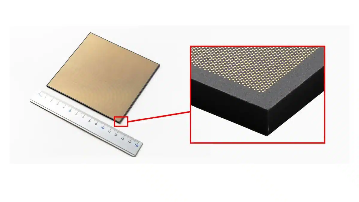
Kyocera has introduced a multilayer ceramic core substrate aimed at advanced AI semiconductor packages such as high‑end xPUs and switch ASICs used in data center and high‑performance compute infrastructure.
The technology focuses on two long‑standing packaging challenges at large substrate sizes: mechanical warpage and fine‑pitch high‑density wiring.
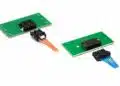
By replacing conventional organic core materials with a rigid multilayer ceramic stack and leveraging through‑ceramic vias formed before sintering, the new substrate class targets more stable assembly yields, slimmer package stacks, and higher routing density for 2.5D integration in AI accelerators and networking silicon.
Key features and benefits
- High rigidity to minimize warpage: The multilayer ceramic core provides significantly higher stiffness than typical organic core materials, helping to suppress bending during reflow and subsequent assembly steps on large package substrates.
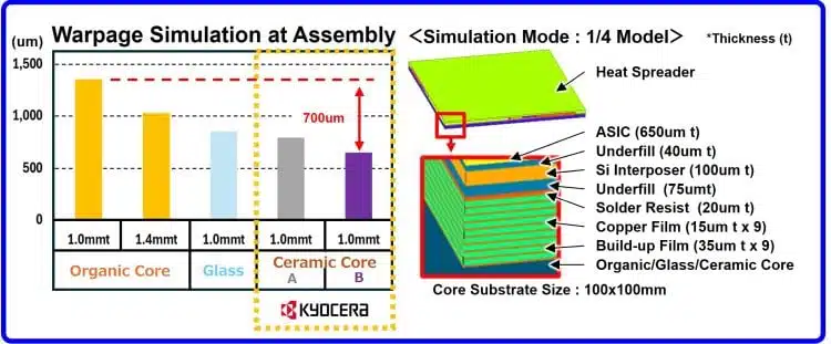
- Support for slim substrate constructions: According to Kyocera’s internal simulations, the higher rigidity enables thinner package substrates while maintaining acceptable flatness, which can be beneficial for thermal path optimization and stack height constraints in dense server systems.
- High‑density three‑dimensional wiring: The multilayer ceramic structure uses vias formed in the green (unfired) ceramic, allowing smaller via diameters and tighter via pitch than mechanically drilled vias in organic cores, which directly supports finer line/space and more aggressive routing strategies.
- Improved reliability of large AI packages: Reducing warpage at large body sizes helps maintain solder joint coplanarity and interconnect integrity for advanced AI processors and switch ASICs with very high bump counts and fine pitch.
- Design‑time simulation support: Kyocera offers thermal, electrical, and warpage simulations for customer designs, allowing package and system engineers to evaluate mechanical and electrical behavior early in the design cycle instead of relying solely on empirical prototyping.
- Customizable substrate design: The ceramic core stack can be tailored to specific device requirements and mounting conditions, allowing optimization for different xPU, ASIC, and interposer configurations.
Typical applications
The multilayer ceramic core substrate is positioned for high‑end semiconductor packages where package size, power density, and interconnect complexity push organic substrates to their limits.
- AI accelerators and xPU devices used in large language model and generative AI workloads in data centers.
- High‑speed switch ASICs and network processors for leaf/spine and core switching in modern cloud and hyperscale infrastructure.
- 2.5D packages where multiple dies (compute, HBM, I/O) are mounted side‑by‑side on a high‑density interposer and require tight control of warpage to maintain bump integrity.
- High‑performance computing (HPC) and custom ASICs with extremely large substrate sizes and very fine bump pitch.
- Potential use in other high‑power, large‑area devices where conventional organic cores struggle with warpage and wiring density, subject to design‑specific evaluation.
Packaging and system‑level context
In current AI servers, many performance and reliability issues originate not only from the die but from the package and board‑level assembly. Large organic core substrates tend to warp under thermal load, which can misalign solder bumps or create local stress points. A stiffer ceramic core can help maintain coplanarity across the entire package body during soldering and operation, which is particularly critical for advanced ball‑grid and micro‑bump arrays.
At the same time, routing the massive number of high‑speed I/Os, power rails, and reference planes needed by AI processors requires extremely fine interconnect structures. The ability to implement high‑density three‑dimensional wiring with small‑diameter vias in a ceramic core is directly relevant here, as it reduces routing congestion and helps maintain signal integrity at increasingly higher data rates.
Technical highlights
The press information highlights several key technical aspects of Kyocera’s multilayer ceramic core substrate, with emphasis on warpage behavior and via technology.
Warpage and rigidity
- The multilayer ceramic core substrate provides greater rigidity than organic core substrates, which helps to minimize warpage during mounting processes such as die attach and board assembly.
- Warpage reduction is particularly important for large semiconductor packages used in AI and networking, where even slight deformation can lead to open or shorted interconnects in dense bump arrays.
- Kyocera’s internal simulations indicate that higher rigidity allows the use of slimmer substrate constructions while maintaining warpage within acceptable limits for assembly. The exact warpage values and thickness ranges are according to the manufacturer’s simulation data and associated datasheets.
High‑density via structure
In multilayer ceramic substrates, conductive connections between layers are implemented using vias formed while the ceramic is still pliable. This differs from the typical drilled or laser‑drilled vias used in organic laminates.
Key via parameters given by Kyocera include:
| Parameter | Value |
|---|---|
| Via diameter | 75 µm |
| Via pitch | 200 µm |
- Forming vias at the green ceramic stage allows more precise micro‑fabrication and smaller via geometries than mechanical drilling, contributing to higher net routing density.
- Smaller via diameters and tighter via pitch help free additional routing channels for high‑speed signals and power distribution, which is essential for xPUs and switch ASICs with very high I/O counts.
- Finer via pitch also supports better breakout from fine‑pitch bump arrays and can reduce the number of routing layers required compared with more coarse organic structures, depending on the design.
2.5D integration focus
The substrate is explicitly targeted at 2.5D packaging, where multiple ICs are mounted side‑by‑side on an interposer or relay substrate with fine circuit patterning.
- In 2.5D packages, warpage control is critical because the interposer or core substrate must maintain flatness across tightly spaced micro‑bumps connecting logic dies and high‑bandwidth memory.
- A rigid ceramic core can improve alignment and mechanical stability, helping to preserve electrical performance over the product lifetime, especially under repeated thermal cycling in data center environments.
Design support and simulation
Kyocera supports customers during the design phase with:
- Thermal simulations to estimate temperature gradients across the substrate and dies under specified power and cooling conditions.
- Electrical simulations to evaluate impedance, signal integrity, and power distribution network behavior for given stackups and routing schemes.
- Warpage simulations that model deformation through various manufacturing and assembly steps, including reflow and different mounting processes.
These simulations allow package and system designers to converge on a substrate configuration that balances electrical performance, thermal management, and mechanical robustness before committing to tooling.
Design‑in notes for engineers
For semiconductor package, module, and system engineers evaluating a transition from organic to ceramic core substrates, several practical points are worth considering.
- Warpage budget and coplanarity: Define a quantitative warpage budget for the entire package across the full thermal profile (from reflow to operation). Use Kyocera’s warpage simulations together with your board‑level simulations to verify that bump and ball coplanarity remain within your assembly limits.
- Substrate thickness versus rigidity: Take advantage of the higher rigidity of the ceramic core to consider thinner overall substrate builds, but validate mechanical margins through both simulation and reliability testing, particularly for large body sizes typical of AI accelerators.
- Via and escape routing strategy: Use the finer via pitch (75 µm diameter, 200 µm pitch) to redesign bump breakout and escape routing for your I/O and power distribution, potentially reducing the number of routing layers or improving signal integrity by shortening paths.
- Thermal path planning: A ceramic core has different thermal conductivity and expansion characteristics compared with organic laminates. Include these properties in your thermal models and in the choice of underfill, lid materials, and heat‑spreader concepts.
- CTE matching and material stackup: Carefully review the coefficient of thermal expansion (CTE) and mechanical properties of the ceramic core relative to the die, underfill, and PCB. Proper CTE matching is key to avoiding stress concentration around solder joints over long‑term thermal cycling.
- Assembly process window: Validate that existing SMT and reflow profiles are compatible with the ceramic substrate stack. Higher rigidity can help, but differences in heat capacity and emissivity may require fine‑tuning to avoid local overheating or solder defects.
- Reliability and qualification: Request detailed reliability data (temperature cycling, thermal shock, power cycling, humidity, and mechanical drop/bend) and, where needed, plan additional qualification focused on large‑body AI and networking packages.
- Electrical performance considerations: Use Kyocera’s electrical simulation support to co‑optimize layer stackups, reference planes, and via structures for high‑speed serial links, ensuring that insertion loss, crosstalk, and impedance discontinuities are within system budgets.
- Supply chain and scalability: For high‑volume AI data center deployments, discuss capacity, lead‑time, and multi‑site manufacturing options early, as ceramic substrate production processes can differ significantly from organic laminates in terms of cycle time and scalability.
From a practical standpoint, design teams should approach the ceramic core substrate as a new packaging platform and plan a structured technology insertion program, including early prototypes, co‑simulation with board and system models, and clear pass/fail criteria for warpage, signal integrity, and reliability.
Source
This article is based on information provided in Kyocera’s official press information and related material about the multilayer ceramic core substrate for advanced semiconductor packages.