




Passive Components Blog
No Result
View All Result
  • Home
  • NewsFilter
    • All
    • Aerospace & Defence
    • Antenna
    • Applications
    • Automotive
    • Capacitors
    • Circuit Protection Devices
    • electro-mechanical news
    • Filters
    • Fuses
    • Inductors
    • Industrial
    • Integrated Passives
    • inter-connect news
    • Market & Supply Chain
    • Market Insights
    • Medical
    • Modelling and Simulation
    • New Materials & Supply
    • New Technologies
    • Non-linear Passives
    • Oscillators
    • Passive Sensors News
    • Resistors
    • RF & Microwave
    • Telecommunication
    • Weekly Digest

    Wk 28 Electronics Supply Chain Digest

    Bourns Introduces Automotive BMS Signal Transformer with Integrated Common Mode Chokes

    Itelcond Introduces High‑Voltage Aluminium Capacitors for Modern IGBT DC‑links

    Bourns Introduces Automotive Shielded Power Inductors for Compact DC‑DC Converters

    EMC Design Fundamentals: Safe Use of Varistors and Common Mode Chokes in Mains and Data-Line Filters

    Murata Unveils Lead Disc Ceramic Capacitors for Automotive Safety and EMI Suppression

    SCHURTER Releases Intelligent Three‑Terminal Fuses for Safer Li‑ion Battery Systems

    Can Copper Conductive Inks Displace Silver in Hybrid Electronics?

    Square-Wave Harmonics and RMS Currents in Power Converters

    Trending Tags

    • Ripple Current
    • RF
    • Leakage Current
    • Tantalum vs Ceramic
    • Snubber
    • Low ESR
    • Feedthrough
    • Derating
    • Dielectric Constant
    • New Products
    • Market Reports
  • VideoFilter
    • All
    • Antenna videos
    • Capacitor videos
    • Circuit Protection Video
    • Filter videos
    • Fuse videos
    • Inductor videos
    • Inter-Connect Video
    • Non-linear passives videos
    • Oscillator videos
    • Passive sensors videos
    • Resistor videos

    EMC Design Fundamentals: Safe Use of Varistors and Common Mode Chokes in Mains and Data-Line Filters

    Ferrite versus Nanocrystalline Power Inductor Cores: Turns, Gap and Size

    KYOCERA AVX Presents Antenna Integrator Studio Tutorial for Antenna Placement and RF Design

    Power Design Simulation Tools for Faster Inductor Selection and Loss Optimization

    EMC‑Compliant PCB and Connector Design Guidelines

    Why Isolated DC/DC Power Supplies Fail Late, Würth Elektronik Podcast

    Designing 800 V DC EMC Filters: Calculation, Simulation and Measurement

    Current Sense Transformer Datasheet and Design‑in Guide

    Designing a USB Type‑C Flyback Planar Transformer with Frenetic’s Planar Tool

    Trending Tags

    • Capacitors explained
    • Inductors explained
    • Resistors explained
    • Filters explained
    • Application Video Guidelines
    • EMC
    • New Products
    • Ripple Current
    • Simulation
    • Tantalum vs Ceramic
  • Knowledge Blog
  • Dossiers
    • AI Hardware Dossier
    • Power Converter Dossier
    • Automotive Dossier
    • Capacitor Dossier
    • Resistor Dossier
    • Inductor Dossier
    • Circuit Protection Dossier
  • Suppliers
    • Who is Who
  • PCNS
    • PCNS 2025
    • PCNS 2023
    • PCNS 2021
    • PCNS 2019
    • PCNS 2017
  • Events
  • Home
  • NewsFilter
    • All
    • Aerospace & Defence
    • Antenna
    • Applications
    • Automotive
    • Capacitors
    • Circuit Protection Devices
    • electro-mechanical news
    • Filters
    • Fuses
    • Inductors
    • Industrial
    • Integrated Passives
    • inter-connect news
    • Market & Supply Chain
    • Market Insights
    • Medical
    • Modelling and Simulation
    • New Materials & Supply
    • New Technologies
    • Non-linear Passives
    • Oscillators
    • Passive Sensors News
    • Resistors
    • RF & Microwave
    • Telecommunication
    • Weekly Digest

    Wk 28 Electronics Supply Chain Digest

    Bourns Introduces Automotive BMS Signal Transformer with Integrated Common Mode Chokes

    Itelcond Introduces High‑Voltage Aluminium Capacitors for Modern IGBT DC‑links

    Bourns Introduces Automotive Shielded Power Inductors for Compact DC‑DC Converters

    EMC Design Fundamentals: Safe Use of Varistors and Common Mode Chokes in Mains and Data-Line Filters

    Murata Unveils Lead Disc Ceramic Capacitors for Automotive Safety and EMI Suppression

    SCHURTER Releases Intelligent Three‑Terminal Fuses for Safer Li‑ion Battery Systems

    Can Copper Conductive Inks Displace Silver in Hybrid Electronics?

    Square-Wave Harmonics and RMS Currents in Power Converters

    Trending Tags

    • Ripple Current
    • RF
    • Leakage Current
    • Tantalum vs Ceramic
    • Snubber
    • Low ESR
    • Feedthrough
    • Derating
    • Dielectric Constant
    • New Products
    • Market Reports
  • VideoFilter
    • All
    • Antenna videos
    • Capacitor videos
    • Circuit Protection Video
    • Filter videos
    • Fuse videos
    • Inductor videos
    • Inter-Connect Video
    • Non-linear passives videos
    • Oscillator videos
    • Passive sensors videos
    • Resistor videos

    EMC Design Fundamentals: Safe Use of Varistors and Common Mode Chokes in Mains and Data-Line Filters

    Ferrite versus Nanocrystalline Power Inductor Cores: Turns, Gap and Size

    KYOCERA AVX Presents Antenna Integrator Studio Tutorial for Antenna Placement and RF Design

    Power Design Simulation Tools for Faster Inductor Selection and Loss Optimization

    EMC‑Compliant PCB and Connector Design Guidelines

    Why Isolated DC/DC Power Supplies Fail Late, Würth Elektronik Podcast

    Designing 800 V DC EMC Filters: Calculation, Simulation and Measurement

    Current Sense Transformer Datasheet and Design‑in Guide

    Designing a USB Type‑C Flyback Planar Transformer with Frenetic’s Planar Tool

    Trending Tags

    • Capacitors explained
    • Inductors explained
    • Resistors explained
    • Filters explained
    • Application Video Guidelines
    • EMC
    • New Products
    • Ripple Current
    • Simulation
    • Tantalum vs Ceramic
  • Knowledge Blog
  • Dossiers
    • AI Hardware Dossier
    • Power Converter Dossier
    • Automotive Dossier
    • Capacitor Dossier
    • Resistor Dossier
    • Inductor Dossier
    • Circuit Protection Dossier
  • Suppliers
    • Who is Who
  • PCNS
    • PCNS 2025
    • PCNS 2023
    • PCNS 2021
    • PCNS 2019
    • PCNS 2017
  • Events
No Result
View All Result
Passive Components Blog
No Result
View All Result

Vishay Introduced Thin Film Submount Platform for Optical and RF Modules

30.4.2026
Reading Time: 8 mins read
A A

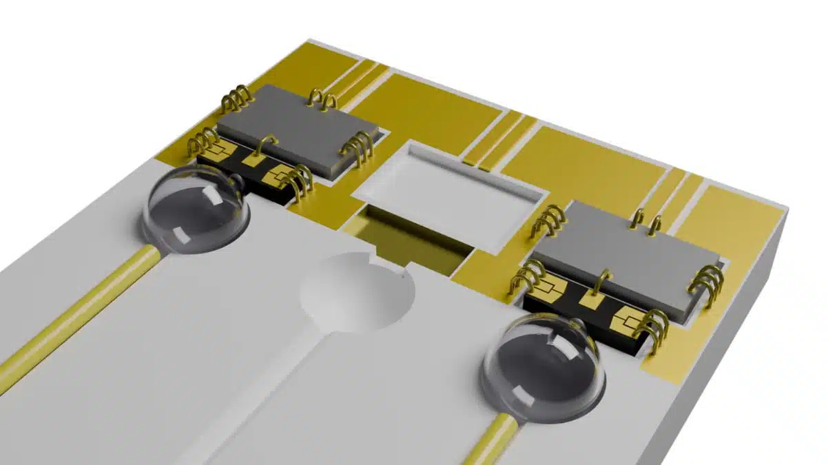
Vishay has introduced a thin film submount platform aimed at high speed optical transceivers, RF modules, and advanced electronic packaging where thermal management, alignment accuracy, and high frequency signal integrity are critical.

The new Vishay platform combines precision thin film passive structures with advanced ceramic substrates such as aluminum nitride to help engineers handle higher power densities and tighter packaging constraints in next‑generation systems.

RelatedPosts

Wk 28 Electronics Supply Chain Digest

Bourns Introduces Automotive BMS Signal Transformer with Integrated Common Mode Chokes

Itelcond Introduces High‑Voltage Aluminium Capacitors for Modern IGBT DC‑links

Introduction

Thin film submounts sit between active devices (for example laser diodes or RF ICs) and the main module or board, providing a mechanically stable, thermally efficient, and electrically optimized interface. Vishay’s new platform extends this concept by combining high thermal conductivity ceramics, precision thin film metallization, and customized machining to support demanding photonics and RF designs in data communications, defense, space, and high reliability industrial markets. According to Vishay, the platform is intended to ease design‑in for both quick‑turn prototyping and volume production.

Key features and benefits

Platform characteristics

  • High thermal conductivity aluminum nitride substrates for efficient heat spreading from high power die into the module structure.
  • Thin film metallization with low loss interconnects to support microwave and millimeter‑wave signal paths.
  • Precision machining of ceramic submounts for tight dimensional control and repeatable mechanical interfaces.
  • Support for integrated passive circuit elements (for example resistors or other thin film features) as part of the submount design.

Manufacturing and logistics

  • Quick‑turn prototyping capabilities combined with high volume production, allowing migration from early samples to series production on the same platform.
  • Production supported from three manufacturing locations, improving supply resilience and logistics planning for global programs.
  • Pre‑deposited AuSn or EPIG finishes available to streamline assembly flows and reduce the number of process steps at the customer side.

Benefits for system design

  • Improved thermal management at the device level, helping to keep junction temperatures under control in high power optical and RF components.
  • Enhanced high frequency performance thanks to low loss thin film interconnects and well‑controlled geometries that reduce parasitics.
  • Better precision alignment of optical elements or RF structures due to tight mechanical tolerances and custom machined features.
  • Reduced manufacturing complexity in final modules because critical interfaces and finishes are already engineered into the submount.

Typical applications

Vishay positions the thin film submount platform primarily for high speed data communications and other high performance modules that must balance power density, signal integrity, and mechanical robustness. Typical application areas include:

  • 800G, 1.6T, and 3.2T optical transceivers, where laser diodes and driver ICs must be cooled efficiently while maintaining precise optical alignment.
  • RF and microwave modules that require low loss transitions and controlled impedance routing at the package level.
  • Millimeter‑wave assemblies for high frequency communications and radar, where thin film structures help manage parasitics and line geometry.
  • Laser diode mounting in industrial, medical, and defense systems, where reliable thermal paths and stable mechanical support are critical.
  • Optical alignment structures in photonics modules, combining mechanical reference features with metallized pads for interconnect.
  • Hermetic packaging solutions and modules that combine wire bonding and SMT processes on a single submount.

Technical highlights

The press release focuses on the submount platform rather than listing fixed part numbers, emphasizing customization around a common thin film and ceramic technology stack. Key technical aspects include:

  • Use of advanced ceramic substrates such as aluminum nitride, selected for high thermal conductivity and good dimensional stability.
  • Precision deposition of passive circuit elements in thin film technology, enabling integrated resistive networks or controlled impedance features directly on the submount.
  • Thin film interconnects engineered for low loss performance at microwave and millimeter‑wave frequencies.
  • Custom geometries and metallization schemes to match specific die layouts, optical paths, or RF transitions.
  • Compatibility with pre‑deposited AuSn solder or EPIG metallization stacks to support different assembly and bonding strategies.

For specific thermal performance figures (for example thermal conductivity values, maximum power dissipation) and electrical parameters, designers should refer to the relevant manufacturer datasheets and application notes for the selected submount configuration according to the manufacturer datasheet.

Platform capabilities overview

AspectDescription
Substrate typeAdvanced ceramics, including aluminum nitride for high thermal performance
Interconnect technologyThin film metallization optimized for high frequency and low loss
Integrated functionsPassive circuit elements and custom routing on the submount
Surface finishesOptions such as pre‑deposited AuSn or EPIG for streamlined assembly
Mechanical customizationPrecision machining for tailored geometries and alignment features

Design flow snapshot

StepRole of the submount platform
Requirement definitionCapture power, frequency, alignment, and assembly constraints
Co‑design with VishayTranslate requirements into geometry, metallization, and finishes
PrototypingQuick‑turn sample builds verify electrical, thermal, and mechanical targets
QualificationTesting under application‑specific environmental conditions
Ramp to productionTransition to high volume at global manufacturing sites

Design‑in notes for engineers

Thermal management

  • Start from junction‑to‑case thermal targets for critical dies and allocate part of the thermal budget to the submount; aluminum nitride and optimized metallization can significantly lower thermal resistance compared to standard alumina structures.
  • Consider the entire thermal path from die attach through submount into the module baseplate or PCB, including solder or TIM layers, when specifying thicknesses and materials.

High frequency layout

  • For RF and millimeter‑wave designs, collaborate early on line impedance, transition geometry, and pad dimensions so that the thin film interconnect layout matches the surrounding PCB and package structures.
  • Use the submount to integrate short controlled impedance runs and critical transitions, reducing parasitics and improving repeatability versus discrete bond wire only solutions.

Opto‑mechanical alignment

  • When designing optical transceivers or laser modules, treat the submount as a key mechanical reference surface; precision machining allows slots, steps, or fiducials that define lens or fiber positions.
  • Specify tolerance requirements for coplanarity, thickness, and feature position to ensure that automated assembly and alignment processes can hit the required optical budgets.

Assembly and metallization choices

  • Select between AuSn solderable surfaces or EPIG finishes based on planned assembly processes (eutectic attach, solder reflow, wire bonding, flip‑chip, or SMT).
  • When combining wire bond and SMT on a single submount, define keep‑out regions, bond pad finishes, and solderable areas clearly to avoid process conflicts.

Reliability and qualification

  • For defense, space, and other high reliability applications, align submount material choices and finishes with the applicable standards and test regimes (temperature cycling, humidity, vibration, outgassing).
  • Validate that CTE (coefficient of thermal expansion) compatibility between die, submount, and carrier structure is sufficient to prevent stress‑related failures over lifetime.

Source

This article is based on information provided in a Vishay Intertechnology press release announcing the Specialty Thin Film thin film submount platform, complemented by related information from Vishay’s specialty thin film capability pages and landing pages.

References

  1. Vishay press release – Thin film submount platform
  2. Vishay Specialty Thin Film – main landing page
  3. Vishay STF miniaturization and precision integration
  4. Vishay STF complex assembly integration
  5. Vishay STF submount platform overview

Related

Recent Posts

Bourns Introduces Automotive BMS Signal Transformer with Integrated Common Mode Chokes

17.7.2026
14

Itelcond Introduces High‑Voltage Aluminium Capacitors for Modern IGBT DC‑links

17.7.2026
25

Bourns Introduces Automotive Shielded Power Inductors for Compact DC‑DC Converters

16.7.2026
39

Murata Unveils Lead Disc Ceramic Capacitors for Automotive Safety and EMI Suppression

15.7.2026
45

SCHURTER Releases Intelligent Three‑Terminal Fuses for Safer Li‑ion Battery Systems

14.7.2026
45

Stackpole Extends Resistance Range of 2512 High‑Power Current Sense Resistors

13.7.2026
29

Littelfuse Announced TVS Diodes for 48 V Automotive Systems

10.7.2026
48

RF Filters and Passive Components Enabling the 7 Missile RF Subsystems

9.7.2026
59

Coilcraft Releases High-Current Ferrite Beads for CISPR 25 EMC compliance

8.7.2026
46

Upcoming Events

Jul 21
16:00 - 17:00 CEST

Safety by design: X and Y Interference suppression capacitors for power line filters

Jul 28
8:00 - 11:00 CEST

Post Procurement Testing of EEE Components for LEO Space Applications

Jul 29
17:30 - 18:30 CEST

To Ferrite or to Nanocrystalline in Transformer Design

View Calendar

Popular Posts

  • Boost Converter Design and Calculation

    0 shares
    Share 0 Tweet 0
  • Buck Converter Design and Calculation

    0 shares
    Share 0 Tweet 0
  • YAGEO Announces July 2026 Capacitor Price Increase

    0 shares
    Share 0 Tweet 0
  • Flyback Converter Design and Calculation

    0 shares
    Share 0 Tweet 0
  • LLC Resonant Converter Design and Calculation

    0 shares
    Share 0 Tweet 0
  • MLCC and Ceramic Capacitors

    0 shares
    Share 0 Tweet 0
  • Earthing Systems and IEC Classification Explained

    0 shares
    Share 0 Tweet 0
  • MLCCs in the Age of AI: Q2 2026 Market Tightness

    0 shares
    Share 0 Tweet 0
  • Nvidia Vera Rubin: Why One AI Rack Needs So Many More MLCC Capacitors

    0 shares
    Share 0 Tweet 0
  • Dual Active Bridge (DAB) Topology

    0 shares
    Share 0 Tweet 0

Newsletter Subscription


Passive Components Blog

© EPCI - Leading Passive Components Educational and Information Site

  • Home
  • Privacy Policy
  • EPCI Membership & Advertisement
  • About

No Result
View All Result
  • Home
  • Knowledge Blog
  • Dossiers
  • PCNS

© EPCI - Leading Passive Components Educational and Information Site

This website uses cookies. By continuing to use this website you are giving consent to cookies being used. Visit our Privacy and Cookie Policy.
Go to mobile version