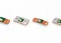
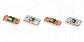





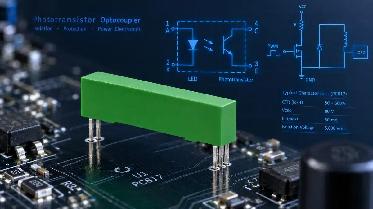
Optical isolators transfer signals across a dielectric barrier using light, keeping high-voltage power stages electrically separated from low-voltage control logic.
A TT Electronics technical white paper Architectural Reliability & Performance Optimization of Optical Isolation sets out a framework for selecting, calculating, and maintaining these components so that isolation stays reliable across the long service life expected in modern power systems. This article summarises the engineering points that matter most when designing optocouplers into smart grid, renewable, and power-conversion hardware.
What the paper covers
The document is a design-oriented technical paper aimed at power system architects rather than a new product launch. It covers the physics of optical coupling, the behaviour of the Current Transfer Ratio (CTR), long-term degradation mechanisms, gate-driver requirements for wide-bandgap designs, and the standards that govern the isolation barrier. Two parts appear as examples: the OPI1268T high-CTR phototransistor isolator and the OPR2100 high-speed optical link.
Galvanic isolation is a performance function here, not only a safety requirement, because a barrier failure can destroy control circuitry and expose personnel to hazardous voltage.
How optical coupling works
Most industrial optoisolators use a gallium arsenide (GaAs) infrared LED as the emitter and a semiconductor photodetector as the receiver. The choice of photodetector defines the component’s role in the system, and the common configurations group by industrial function.
| Photodetector type | Key components | Primary application | Strategic value |
|---|---|---|---|
| Phototransistor | LED + bipolar transistor | SMPS feedback loops | High gain, cost-effective DC signal isolation for general logic |
| Photodiode | LED + photodiode | High-speed data / IEDs | Minimal propagation delay for real-time grid monitoring |
| Photo-Darlington | LED + Darlington pair | Low-power detection | Very high CTR for sensitive triggering at low current |
| Photo-SCR / TRIAC | LED + thyristor / triac | AC load and motor control | Zero-crossing detection and high dv/dt noise rejection |
| Isolation amplifier | LED + sigma-delta IC | Voltage / current sensing | High-linearity analog sensing for grid state estimation |
Physical construction sets the insulation limit. Planar or sandwich layouts are typically used below 2.5 kV, while “silicone dome” construction, in which the LED and sensor are encapsulated in a transparent dome to lengthen the dielectric path, is used for higher-voltage environments in the 2.5 kV to 6 kV range.
Current Transfer Ratio and worst-case design
CTR is the ratio of output collector current to input LED forward current, expressed as a percentage:
%
CTR is the most important and most challenging design parameter because it varies with production tolerance (managed through binning), temperature, and forward current, and is non-linear even within a bin. The safe approach is to design against a calculated worst case rather than the nominal datasheet figure.
Worked example. For a Bin C device rated 200–400% at 5 mA and 25 °C, operated instead at 2 mA and 80 °C:
- Minimum Bin C CTR: 200%
- Current scaling factor () for 2 mA: 0.76 (per application note ANO007)
- Temperature scaling factor () for 80 °C: 0.85
- Effective CTR: 200% × 0.76 × 0.85 = 129.2%
For design engineers, this means a logic-high threshold verified only against the nominal 200% figure could fail to trigger during summer peak temperatures or low-power standby, where forward current is reduced. For feedback loops, the small-signal (AC) CTR defined by the slope of collector current versus forward current must be used instead of the DC value. Engineers working on isolated converters will recognise this dependency from flyback feedback-loop compensation, where the optocoupler is part of the loop.
Reliability and CTR degradation over service life
In assets built for a 25-year lifecycle, LED ageing is a primary failure mode. As the GaAs LED’s light output falls over time, CTR degrades directly. The mechanism is electromigration and crystal-defect formation in the LED junction: high current density drives atomic diffusion, creating non-radiative recombination centres that reduce quantum efficiency.
Long-term behaviour is predicted from accelerated stress testing using the Black equation for the acceleration factor, with an activation energy of 0.7 eV and the Boltzmann constant of 8.617 × 10⁻⁵ eV/K. Statistical margin matters: while the average CTR drop after simulated ~25-year testing is about 5%, the lowest 5% of the population may fall to roughly 87% relative CTR, so the design target should be the “average − 2σ” case to cover 95% of the population.
See more details about the reliability calculation in the referenced white paper.
Design-in notes for engineers
Practical measures to extend optocoupler service life:
- Reduce the effective LED-on duty cycle to lower cumulative electron flow and slow crystal-defect formation.
- Minimise forward current (I_F) to the lowest viable level for reliable logic detection, which extends mean time to failure.
- Improve thermal management with large vias and dedicated pads; every 10 °C reduction can roughly double LED lifespan.
- Eliminate peak transient currents through filtering, since spikes accelerate electromigration.
- Apply burn-in on mission-critical hardware to remove infant-mortality failures and stabilise junctions.
- Budget for CTR loss by assuming degradation of up to 50% over 25 years.
Treat the optocoupler as a power component with a defined thermal path rather than as a simple signal part.
Wide-bandgap gate drivers
The move to silicon carbide (SiC) and gallium nitride (GaN) enables 1500 VDC bus voltages but adds high switching noise, so “smart” isolated gate drivers are needed to manage these environments. The relevant features are common-mode transient immunity (CMTI) above 100 kV/µs to prevent false switching from high dv/dt, desaturation (DESAT) detection to trigger a soft shutdown within nanoseconds of a short circuit, and active Miller clamping to prevent parasitic turn-on.
Two implementation approaches compare as follows, without quantitative benchmark data:
| Metric | Discrete driver approach | Integrated smart gate driver |
|---|---|---|
| Component count | High (logic + isolators) | Low (monolithic package) |
| Response time | Limited by multiple IC delays | Targeted at under 100 ns |
| Footprint | Larger PCB area | Compact, high-density |
| Reliability | Higher system-level failure risk | Higher MTBF through integration |
Standards and the isolation barrier
Product-level Hipot tests alone are not sufficient. IEC 61010-1 verifies only a one-minute withstand voltage, whereas component standards such as IEC 60747-5-5 and VDE 0884-17 address the barrier’s long-term health. Partial-discharge testing is the meaningful measure of dielectric integrity: under IEC 60747-5-5, discharge must remain below 5 pC at 1.5 to 1.875 times the rated working voltage, confirming the absence of microscopic voids that could erode breakdown over decades.
User-touchable interfaces call for reinforced insulation. Optical isolators offer a barrier thickness of roughly 100–400 µm compared with about 7–30 µm for digital isolators. If you are weighing optical against digital isolation options, that barrier-thickness difference is one factor among several to evaluate against your insulation requirements.
What to validate before design release
- Confirm the specific CTR bin, scaling factors, and rated conditions in the current datasheet, since the values above are illustrative rather than a full specification.
- Verify VDE and UL certificates for the required insulation class of the exact part number chosen.
- Recheck the worst-case CTR against your actual forward current, temperature range, and end-of-life margin.
- Confirm partial-discharge and working-voltage ratings against your operating, surge, fault, and transient conditions.
- Full electrical ratings, dimensions, and qualification data for individual part numbers are not specified here; confirm these in the current datasheet before schematic, layout, or production release.
Further reading
- Mastering Galvanic Isolation in Power Electronics
- Feedback Loop Compensation of Current-Mode Flyback Converter
Source
This article is based on a technical white paper published by TT Electronics on the architectural reliability and performance optimisation of optical isolation in modern power systems. The values and examples cited here are drawn from that document; engineers should consult the current manufacturer datasheet and qualification documentation for final component selection, qualification, and design release.
References
- More details and pdf download available from TT Electronics — Architectural Reliability & Performance Optimization of Optical Isolation (white paper)