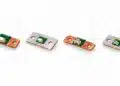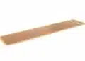
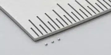




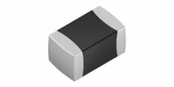
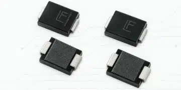



Knowles has introduced the ATT A-Series, a surface-mount RF attenuator family for broadband signal chains from DC to 20 GHz.
The Knowles launch adds a compact, 50 Ω matched attenuator option for designs where controlled signal reduction, thermal handling and board area must be considered together.
Key features and benefits
- Precision thin-film resistor technology on a ceramic substrate.
- DC to 20 GHz frequency coverage.
- Standard attenuation values from 0 dB to 20 dB.
- 50 Ω matched RF input and output ports.
- Surface-mount package measuring 2.03 × 1.65 × 0.30 mm.
- Power handling up to 6.5 W continuous-wave at 100 °C.
- Operating temperature range of −55 °C to +125 °C.
- MSL 1 and SMT assembly compatibility.
- The product announcement describes pin compatibility with existing industry-standard chip attenuators, although the publicly accessible documentation reviewed does not provide the land pattern, compatible competitor footprints, or part-by-part pinout information needed to confirm a drop-in replacement.
The published family name is ATT A-Series. The product finder identifies the package-level designation ATTA080. No individual orderable part numbers, attenuation-specific suffixes, tolerance values, return-loss limits, attenuation-flatness limits, insertion-loss data, S-parameters, outline drawing, recommended land pattern, reliability report or qualification report were publicly accessible in the documentation reviewed.
Technical highlights
| Parameter | Value | Notes |
|---|---|---|
| Series | ATT A-Series | RF attenuators |
| Product designation | ATTA080 | Product finder entry |
| Frequency range | DC to 20 GHz | Broadband operation |
| Attenuation range | 0 dB to 20 dB | Standard values |
| Characteristic impedance | 50 Ω | Matched RF ports |
| Power handling | Up to 6.5 W CW | At 100 °C |
| Operating temperature | −55 °C to +125 °C | Published range |
| Package size | 2.03 × 1.65 × 0.30 mm | 0.080 × 0.065 × 0.012 in. |
| Assembly status | MSL 1 | SMT compatible |
An attenuator in this class is a controlled resistive network rather than a generic chip resistor. Its practical role is to establish a known signal level, isolate stages, improve impedance conditions or protect a more sensitive circuit block from excessive RF power. In a wideband chain, the component should be assessed as an RF structure with package parasitics, PCB launch geometry and transmission-line impedance included in the analysis. Resistor Technology Selection and Benchmark Guidelines
The 6.5 W CW figure is specified at 100 °C. It should therefore not be treated as a universal board-level rating. The final usable dissipation depends on the actual local temperature, copper area, thermal path, mounting conditions, signal waveform and duty cycle. The current public material does not provide a derating curve, thermal resistance, pulsed-power rating or temperature-dependent power limit.
Typical applications
The released documentation identifies radar, electronically steered phased-array antennas, electronic support measures, transmit/receive modules, wireless infrastructure, satellite communications, and RF test and measurement equipment.
| Application | Supported published attributes | Circuit role |
|---|---|---|
| Radar and phased arrays | DC–20 GHz, 50 Ω ports, compact SMT package | Interstage level setting |
| T/R modules | 6.5 W CW at 100 °C, −55 °C to +125 °C | Gain staging or interface attenuation |
| ESM receivers | DC–20 GHz, standard 0–20 dB values | Signal-level control |
| Wireless infrastructure | 50 Ω matching, SMT assembly | RF path matching and level trim |
| SATCOM equipment | DC–20 GHz, compact outline | Broadband module integration |
| RF test equipment | 0–20 dB attenuation range, 50 Ω ports | Fixed attenuation and port conditioning |
The published frequency range and 50 Ω matching support use in broadband RF paths where attenuation is required without changing the intended system impedance. The compact 2.03 × 1.65 mm footprint is relevant to multi-channel assemblies, including phased-array tiles and dense RF modules, where repeated signal-conditioning functions consume substantial board area.
The announcement also identifies defence, aerospace, industrial and communications assemblies as target markets. However, no public AEC-Q200, MIL qualification, space-grade screening, humidity-bias, endurance or ESD test report was found in the reviewed documents. A stated end market should not be read as proof of a particular qualification level.
Application fit
In a receiver chain, a fixed attenuator can be placed between gain stages to improve level management and reduce the risk of overdriving a following amplifier or mixer. In a transmit/receive module, it can establish a defined interface level between functional blocks, subject to verification of dissipation under the maximum RF power and temperature profile.
For multichannel radio systems, repeatable attenuation and 50 Ω interfaces can help maintain predictable signal conditions between channels. This does not replace full network validation: return loss, attenuation flatness, phase effect, power compression of adjacent active devices and PCB launch performance must be verified across the operating band.
The standard 0 dB to 20 dB range may also be useful where an attenuation position is retained for design flexibility. A 0 dB version can preserve the mechanical and RF footprint while allowing later attenuation changes, but the public sources reviewed do not provide attenuation tolerances, frequency-dependent flatness, phase data or part-number ordering details. Those parameters should be confirmed in the current datasheet before fixing gain budgets or production BOMs.
Design-in notes for engineers
- Confirm the exact attenuation value, orderable part number and frequency-dependent attenuation limit from the current datasheet before release.
- Check return loss and S-parameters using the final PCB stack-up, launch geometry and intended reference planes. No public S-parameter files or RF curves were located during this review.
- Treat the 6.5 W CW value as a condition-specific rating at 100 °C, not as a direct indication of permitted dissipation at another ambient or case temperature.
- Evaluate local copper area, via stitching, substrate thermal conductivity and adjacent heat sources before selecting the package for a high-power position.
- Verify RF voltage and current stress within the internal resistive network for the actual attenuation value, frequency, impedance mismatch and VSWR condition.
- Review the solder land pattern, reflow process and package outline in the current manufacturer documentation. Publicly accessible material reviewed for this article does not include an outline drawing or mounting guideline.
- Confirm whether the required attenuation is a fixed value, a tuned production option or a custom value. Knowles states that custom attenuation values, power ratings and specialised configurations are available, but no public configuration limits were found.
- Do not assume the claimed industry-standard pin compatibility covers every existing chip attenuator footprint. Verify pad geometry, orientation, RF launch and electrical performance directly against the intended replacement part.
- A full component-level and system-level validation remains necessary before schematic, layout or production release.
Further reading
- Resistor Technology Selection and Benchmark Guidelines
- Resistor Network
- Resistor Symbols
- Modelithics Releases COMPLETE Library v26.2 for Keysight Genesys
Source
This article is based on the Knowles ATT A-Series launch material and official RF/microwave product documentation. Engineers should consult the current manufacturer datasheet and supporting documentation for final part selection, qualification review, RF modelling, PCB layout and design release.