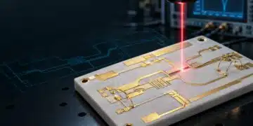


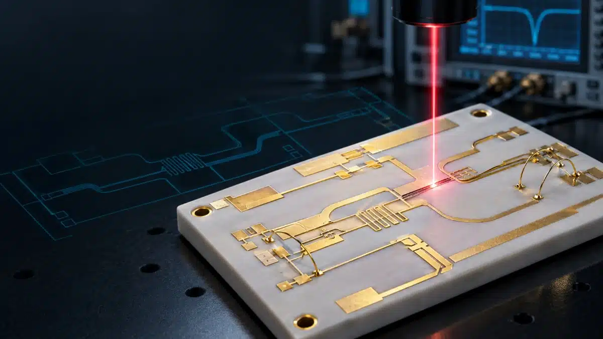
Heraeus Electronics has presented laser etching as a direct-write patterning method for RF circuits made with its C5735 thick-film gold conductor paste.
The Heraeus Electronics development is relevant to hybrid circuits and fine-feature passive structures where conductor geometry, wire-bond compatibility, and RF layout can be as important as the nominal value of an individual passive component.
Key features and benefits
C5735 is a Pb-, Ni- and Cd-free gold conductor paste for thick-film processing and Al or Au wire-bonding applications. It produces a dense fired film and supports screen-printed lines and spaces down to 75 µm; etching can extend the feature size down to 25 µm.
- Direct-write laser etching removes gold selectively after thick-film processing, avoiding photomask preparation in the patterning step.
- The release describes line and space capability below 1 mil; the current C5735 product information gives ultra-fine etched features down to 25 µm.
- Laser patterning can support rapid prototype changes because the pattern is digitally defined rather than transferred through a new mask.
- The process is relevant where conductor width, spacing, edge definition, and layout repeatability influence RF impedance and parasitic coupling.
- The announced process concerns conductive metallization for hybrid circuits, not a new discrete resistor, capacitor, inductor, or EMI-filter series.
The main relevance for passive components lies in hybrid and integrated implementations: printed conductor patterns can form interconnects, contact structures, inductive geometries, transmission-line sections, resistor-network connections, and other RF passive circuit features on a ceramic or similar substrate.
Technical highlights
| Parameter | Value | Notes |
|---|---|---|
| Material | C5735 | Gold conductor paste |
| Bonding use | Al or Au wire | Product-page application |
| Restricted metals | Pb, Ni, Cd free | Product-page statement |
| Screen-printed features | 75 µm | Lines and spaces |
| Etched features | 25 µm | Ultra-fine features |
| Laser-etched features | <1 mil | Release-only claim |
The <1 mil figure in the release is consistent in scale with the 25 µm etched-feature figure published on the current C5735 product page, but the public materials reviewed do not provide a laser-process datasheet, dimensional tolerance, process window, surface-roughness data, RF loss data, or production-yield specification for the laser-etched result.
C5735 is a conductor paste, rather than a resistor paste or dielectric paste. Its use in passive-component manufacturing is therefore indirect but technically meaningful: it can provide the conductive patterning used alongside fired resistor, dielectric, or other thick-film functional layers in hybrid circuits and custom passive networks.
Applicability for passive components
The most direct fit is with thick-film resistor technology and hybrid-circuit manufacturing. Conventional thick-film chip resistors use a fired resistive cermet layer, conductive terminations, laser trimming, protective passivation, and external solderable terminations. C5735 is not presented as a replacement for the resistive cermet layer or for final-value laser trimming of standard chip resistors.
Its potential role is instead in the surrounding conductive architecture:
- Fine-pitch conductor traces and bond pads in RF hybrid assemblies
- Printed resistor networks and hybrid modules requiring fine conductor separation
- RF matching, attenuation, termination, and sensor-interface circuits where layout parasitics must be controlled
- Custom passive structures on ceramic substrates, including conductor-defined sections around resistive or dielectric functional areas
- Wire-bonded high-reliability circuits using Al or Au wire
| Passive-component area | Relevance | Published support |
|---|---|---|
| Standard chip resistors | Indirect | Conductor patterning only |
| Thick-film resistor networks | Moderate | Thick-film circuit architecture |
| RF passive hybrids | Strong | Fine etched conductor features |
| Wire-bonded RF modules | Strong | Al or Au wire bonding |
| MLCC production | Not established | No MLCC documentation reviewed |
| Power inductors | Not established | No magnetic-component documentation reviewed |
| EMI filters | Indirect | RF layout, not filter ratings |
The public release identifies RF applications, but it does not provide electrical ratings, characteristic impedance data, insertion-loss curves, S-parameters, current capability, temperature range, qualification status, or application-specific reliability data for laser-etched C5735 circuits. Those omissions mean the technology should not yet be specified for a defined filter, matching network, attenuator, or high-power RF path solely from the published article.
Typical applications
Fine conductor definition becomes increasingly significant when a circuit’s physical geometry controls electrical behaviour. In RF hybrids, trace width, trace spacing, substrate properties, metal thickness, via layout, bond-wire geometry, and adjacent conductor placement can all influence impedance, coupling, loss, and repeatability.
The documented 25 µm etched-feature capability makes the technology relevant for fine-pitch metallization patterns in:
- RF hybrid circuits where compact conductor routing and spacing are required
- Ceramic-based resistor networks and custom passive assemblies
- Wire-bonded circuits using Al or Au interconnects
- High-reliability electronics where gold metallization and bondability are part of the assembly strategy
- Prototype and low-to-mid-volume circuit development where avoiding a new photomask can shorten layout iterations
Heraeus positions thick-film materials for automotive, industrial, military, consumer, and hybrid-circuit applications. However, the reviewed C5735 documentation does not establish AEC-Q200 qualification, military qualification, defined operating-temperature limits, or application-specific environmental performance for this particular material and laser-etching process.
Design-in notes for engineers
- Treat laser-etched C5735 as a process and materials option, not as a catalogue passive component with a finished electrical specification.
- Obtain the current C5735 technical datasheet before committing to material selection, firing conditions, printed thickness, sheet resistance assumptions, adhesion, solderability, or wire-bond process parameters.
- Request RF characterisation for the intended substrate stack-up, conductor thickness, line geometry, frequency range, and termination method. A minimum feature size alone does not establish impedance control or insertion loss.
- Check whether laser removal creates edge roughness, redeposited debris, local substrate effects, or changes in bond-pad quality under the planned laser wavelength and pulse conditions.
- Validate wire-bond pull strength, shear strength, and RF performance after laser processing where Al or Au bonding is used.
- Compare the total process flow with chemical etching, including mask cost, setup time, throughput, material yield, inspection needs, post-process cleaning, and laser capital cost.
- Confirm compatibility with downstream resistor, dielectric, passivation, soldering, and encapsulation processes in a multi-layer thick-film circuit.
- This does not replace system-level validation. RF behaviour must be measured on the final substrate, package, PCB transition, and assembly configuration.
For RF and high-frequency resistor applications, component parasitics and PCB layout can dominate nominal resistance at higher frequencies. The same principle applies more broadly to hybrid passive structures: conductor geometry must be assessed together with substrate dielectric properties, metallization thickness, bond wires, package transitions, and the final mounting environment.
Further reading
- Thick-Film Chip Resistors: Construction, Properties, Selection and Design Guide
- SMD Chip Resistors: Types, Packages, Ratings and Selection
- Thin Film and Metal Film Resistors
- Resistor Types and Construction Fundamentals
Source
This article is based on the Heraeus Electronics laser-etching release and official C5735 thick-film materials documentation. Engineers should consult the current manufacturer datasheet, applicable process documentation, and application-specific qualification evidence before final material selection, layout release, or production approval.