Passive Components Blog
No Result
View All Result
  • Home
  • NewsFilter
    • All
    • Aerospace & Defence
    • Antenna
    • Applications
    • Automotive
    • Capacitors
    • Circuit Protection Devices
    • electro-mechanical news
    • Filters
    • Fuses
    • Inductors
    • Industrial
    • Integrated Passives
    • inter-connect news
    • Market & Supply Chain
    • Market Insights
    • Medical
    • Modelling and Simulation
    • New Materials & Supply
    • New Technologies
    • Non-linear Passives
    • Oscillators
    • Passive Sensors News
    • Resistors
    • RF & Microwave
    • Telecommunication
    • Weekly Digest

    Samsung Electro-Mechanics High Capacitance MLCCs for ADAS SoCs

    Murata Expands its Automotive Common Mode Choke Coils to 150C and High Current Capability

    Bourns Releases New Current Transformer

    Skeleton Releases GrapheneGPU to Reduce AI Energy Consumption by 44% and Boosts Power by 40%

    VINATech Expands Aluminum Capacitor Portfolio with Acquisition ofย Enesol

    binder Offers Wide Range of M12 Panel Mount Connectors

    Bourns Releases New Shielded Power Inductors for DDR5

    Supercapacitors Benefits in Industrial Valve Fail-Safe Control Systems

    Wk 21 Electronics Supply Chain Digest

    Trending Tags

    • Ripple Current
    • RF
    • Leakage Current
    • Tantalum vs Ceramic
    • Snubber
    • Low ESR
    • Feedthrough
    • Derating
    • Dielectric Constant
    • New Products
    • Market Reports
  • VideoFilter
    • All
    • Antenna videos
    • Capacitor videos
    • Circuit Protection Video
    • Filter videos
    • Fuse videos
    • Inductor videos
    • Inter-Connect Video
    • Non-linear passives videos
    • Oscillator videos
    • Passive sensors videos
    • Resistor videos

    Coupled Inductors Circuit Model and Examples of its Applications

    Inductor Resonances and its Impact to EMI

    Highly Reliable Flex Rigid PCBs, Wรผrth Elektronik Webinar

    Causes of Oscillations in Flyback Converters

    How to design a 60W Flyback Transformer

    Modeling and Simulation of Leakage Inductance

    Power Inductor Considerations for AI High Power Computing โ€“ Vishay Video

    Coupled Inductors in Multiphase Boost Converters

    VPG Demonstrates Precision Resistor in Cryogenic Conditions

    Trending Tags

    • Capacitors explained
    • Inductors explained
    • Resistors explained
    • Filters explained
    • Application Video Guidelines
    • EMC
    • New Products
    • Ripple Current
    • Simulation
    • Tantalum vs Ceramic
  • Knowledge Blog
  • Suppliers
    • Who is Who
  • Events
No Result
View All Result
Passive Components Blog
No Result
View All Result

RC Snubber Design for SMPS Protection Part II

24.8.2022
Reading Time: 12 mins read
A A

Source: In Compliance Mag article

by Bogdan Adamczyk and Bill Spence

RelatedPosts

Snubber Capacitors Functionality and Selection Guide

TDK Releases its Application Guide on Motor/Inverter Circuit Configuration

What Ceramic Technologies Are Best for High Power Density Applications?

Part II: Design Process and Verification

This part II of the RC Snubber topic discusses the systematic and efficient design process and design verification through simulations and laboratory measurements (see [1] for Part I โ€“ fundamentals of inductive switching and RC snubber impact).

Design Process

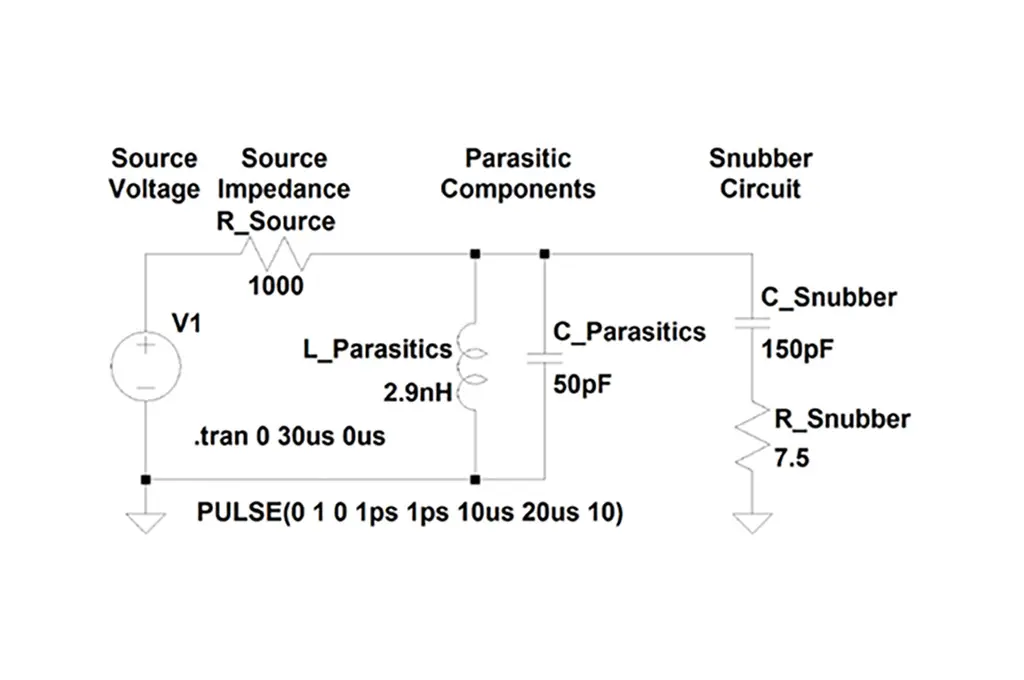
Figure 1 shows the LC resonant circuit with an RC snubber discussed in Part I [1].

Featured Figure 1: LC parasitic circuit with the RC snubber

In this part we discuss a systematic and efficient design process leading to the choice of the snubberโ€™s capacitor and resistor values shown in Figure 1.

The resonant frequency formula for a circuit without the snubber is [1]

 (1)

The purpose of using the RC snubber is to suppress the ringing and move the ringing frequency to a lower value (often 50% or less of the original value). Note that in order to half the ringing frequency in Eq. (1), the term under the square root needs to quadruple. If we keep the inductance parasitics constant, the quadruple of the capacitive component can be accomplished by

  (2)

where

  (3)

Now the total circuit capacitance, C, is four times the original parasitic capacitance value.

  (4)

The traditional RC snubber design process consists of the following steps:

Measure the ringing frequency at the switching node,โ€Š fr

Add a capacitor, CADD, from the switching node to the reference node

Measure the resulting (lower) ringing frequency, frโ€Šโ€˜

Keep changing the added capacitorโ€™s value until the ringing frequency frโ€Šโ€˜ is approximately half of the original ringing frequency, fr, without the added capacitor

This last CADD is the minimum value for the snubber capacitance, Csnub.

Calculate Cโˆ‘parasitics

  (5)

Calculate Lโˆ‘parasitics

  (6)

Finally, calculate Rsnub, [2],

  (7)

Note that this traditional design process requires the substitution of capacitor snubber values to discover CADD by halving fr. This can be easily done in simulations, but not in the actual measurements. The constant changing of capacitor values, hunting for the particular value, is time consuming and can be destructive.

A faster and more practical method is to try a single capacitor value to determine the circuitโ€™s parasitic capacitance. This process consists of the following steps:

Measure the ringing frequency at the switching node,

Add a capacitor, CADD, from the switching node to the reference node. Pick a value between 47pF and 100pF as a starting point

Measure the resulting (lower) ringing frequency, frโ€Šโ€˜

Calculate Cโˆ‘parasitics

  (8)

Calculate Lโˆ‘parasitics

  (9)

Calculate Csnub,min, [3],

  (10)

Finally, calculate Rsnub

  (11)


Design Verification through Simulations

The unsnubbed circuit is shown in Figure 2(a) with the resonant frequency, fr = 412.6 MHz, shown in Figure 2(b), (Step 1).


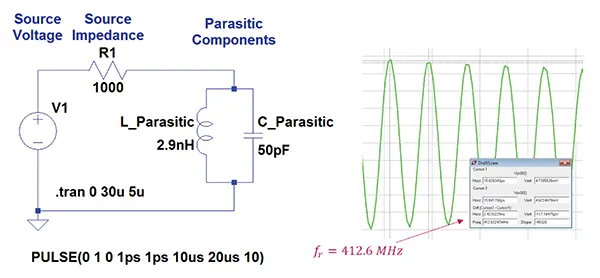
Figure 2(a) shows the circuit with the added capacitance CADD = 100pF with the resonant frequency,
fr = 412.6 MHz, shown in Figure 2(b), (Step 2 and 3).

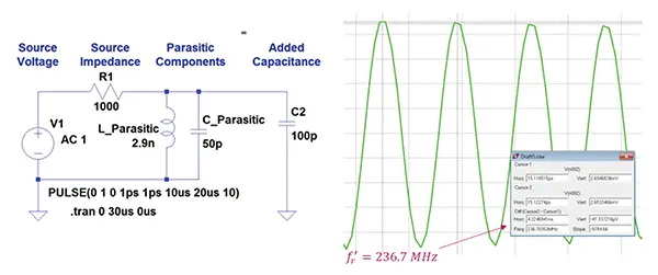
Figure 3: (a) Circuit with added capacitance, (b) resonant frequency


Step 4. Calculate C
โˆ‘parasitics

Step 5. Calculate Lโˆ‘parasitics

Step 6. Calculate Csnub,min

Step 7. Calculate Rsnub

These resulting C and R values were implemented in the RC snubber shown in Figure 1. The simulated ringing waveforms for this circuit were discussed in Part I [1], and are repeated here in Figure 4.

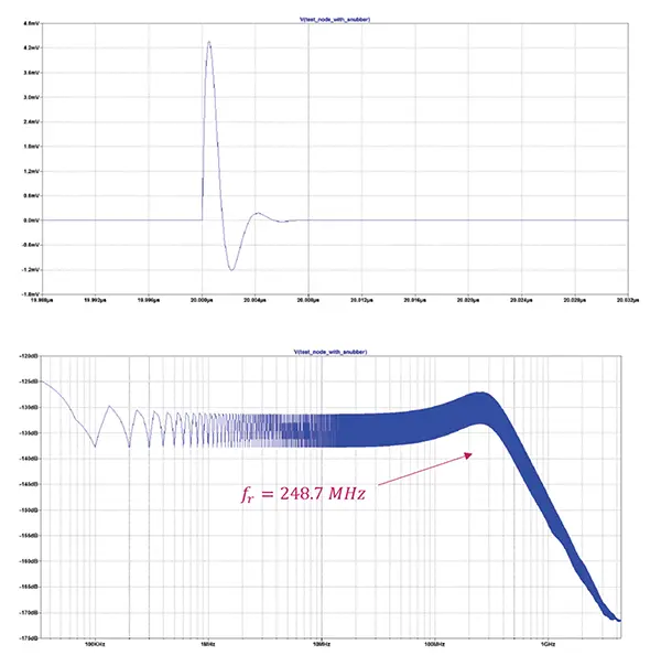
Figure 4: Ringing waveforms with a snubber added: (a) close-up of a time domain waveform, (b) FFT of the waveform

Note that the new ringing frequency of 248.7 MHz is much lower than the original ringing frequency of 412.6 MHz, of the unsnubbed circuit.

Design Verification through Measurements

In this section we follow the design process of the previous section with the values obtained from measurements (instead of the simulated values).

Figure 5 shows a (redacted) circuit schematic of a buck SMPS with the designed snubber.

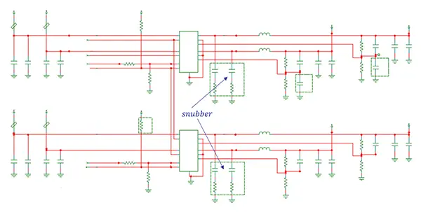
Figure 5: Buck SMPS with a snubber


Figure 6 shows the actual PCB and a differential probe used for measurements [4].

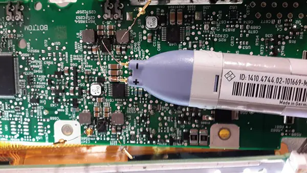
Figure 6: Actual PCB and a differential probe

Figure 7 shows the ringing waveform corresponding the un-snubbed circuit. The measured ringing frequency is fr = 476.1 MHz (Step 1).

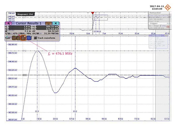
Figure 7: Unsnubbed SMPS: voltage at the switching node


Next, a 68 pF capacitor is added (Step 2). The resulting ringing waveform is shown in Figure 8.

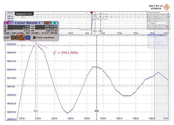
Figure 8: Voltage at the switching node with a C= 68 pF capacitor added


The new (lower) ringing frequency is frโ€˜ = 294.1 MHz (Step 3).

Step 4. Calculate Cโˆ‘parasitics

Step 5. Calculate Lโˆ‘parasitics

Step 6. Calculate Csnub,min

Step 7. Calculate Rsnub

Figure 9 shows the voltage waveform with the C = 150 pF snubber added.

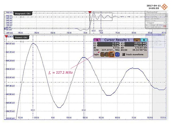
Figure 9: Voltage at the switching node with a C = 150 pF snubber added

Note the decrease in the ringing frequency. Finally, a full RC snubber is implemented (Csnub = 150 pF, Rsnub = 7.5 ฮฉ). The resulting waveform is shown in Figure 10.

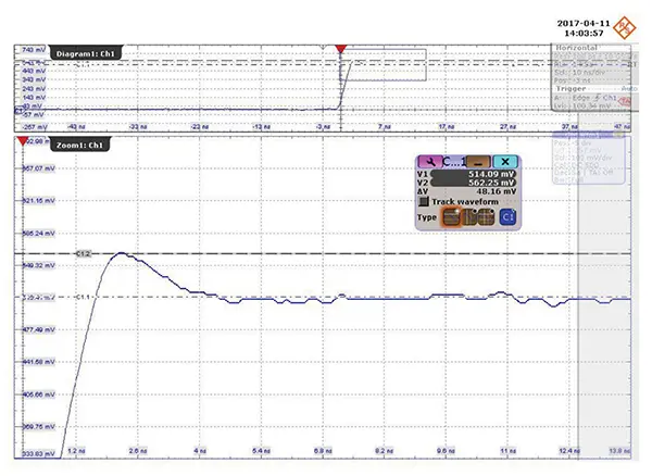
Figure 10: Voltage at the switching node with a full RC snubber added


It is evident that the full RC snubber suppressed the ringing at the switching node.


Final Conclusions

It is worth repeating that parasitic inductance in the circuit is distributed over the entire PCB and includes the package inductances. While the snubber components are calculated assuming their effective values, there is no way to physically put them in the circuit to provide ideal damping. The best way to reduce overshoots and ringing is to actually minimize the undesirable inductances in the circuit with good layout practices. Choosing the right low side FETs with low inductance packages and/or integrated Schottky body diodes will offer additional benefits.

Finally, these equations will get you into the ballpark. Differences in leading edge and trailing edge ringing will result in Snubber Circuit component compromises.

Continue reading:

  • RC Snubber Design for SMPS Protection Part I
  • Filtering Capacitors for Switch Mode Power Supplies
  • Guide to Snubber


References

  1. Bogdan Adamczyk, Bill Spence, โ€œRC Snubber Design for SMPS Protection โ€“ Part I: Fundamentals of Inductive Switching and RC Snubber Impact,โ€ In Compliance Magazine, January 2019.
  2. Jeff Falin, โ€œMinimizing Ringing at the Switch Node of a Boost Converter,โ€ Texas Instruments Application Report SLVA255, September 2006.
  3. Havanur, Sanjay, Application Note AN100-1, Alpha & Omega Semiconductor, May 2007.
  4. Bill Spence, โ€œSnubber Design: Reducing SMPS EMI,โ€ Lunch and Learn, Gentex Corp., 2014.

Dr. Bogdan Adamczyk is a professor and the director of the EMC Center at Grand Valley State University (http://www.gvsu.edu/emccenter) where he performs research and develops EMC educational material. He is an iNARTE certified EMC Master Design Engineer, a founding member and the chair of the IEEE EMC West Michigan Chapter. Prof. Adamczyk is the author of the textbook โ€œFoundations of Electromagnetic Compatibility with Practical Applicationsโ€ (Wiley, 2017). He can be reached at [email protected].

William Spence is a Senior Electromagnetic-Compliance Engineer and has been working in Gentex Corporationโ€™s Electro-Magnetic-Engineering Lab for the last fifteen years. Previously, Bill was a Senior Microphone Design Engineer at Electro-Voice, Inc., where he worked for twenty-four years. Billโ€™s name has been listed in a dozen U.S. Patents for automotive microphone, digital communications, and switch-mode-power-supply designs. He frequently presents seminars on EMC/ESD topics and microphone design. Bill can be reached at [email protected].

Related

Recent Posts

Samsung Electro-Mechanics High Capacitance MLCCs for ADAS SoCs

30.5.2025
7

Murata Expands its Automotive Common Mode Choke Coils to 150C and High Current Capability

29.5.2025
7

Bourns Releases New Current Transformer

29.5.2025
10

Skeleton Releases GrapheneGPU to Reduce AI Energy Consumption by 44% and Boosts Power by 40%

29.5.2025
26

VINATech Expands Aluminum Capacitor Portfolio with Acquisition ofย Enesol

28.5.2025
48

Bourns Releases New Shielded Power Inductors for DDR5

29.5.2025
20

Supercapacitors Benefits in Industrial Valve Fail-Safe Control Systems

26.5.2025
27

Samsung Electro-Mechanics Releases High-Capacitance MLCCs for AI Server Applications

21.5.2025
54

Samsung Electro-Mechanics Releases 165C Automotive 0806 Size Power Inductors

21.5.2025
29

Coupled Inductors Circuit Model and Examples of its Applications

21.5.2025
74

Upcoming Events

Jun 4
11:00 - 12:00 CEST

Wรผrth Elektronik PCB Production in Asia

View Calendar

Popular Posts

  • Buck Converter Design and Calculation

    0 shares
    Share 0 Tweet 0
  • Boost Converter Design and Calculation

    0 shares
    Share 0 Tweet 0
  • SEPIC Converter Design and Calculation

    0 shares
    Share 0 Tweet 0
  • Flyback Converter Design and Calculation

    0 shares
    Share 0 Tweet 0
  • Filter Q Factor Explained

    0 shares
    Share 0 Tweet 0
  • LLC Resonant Converter Design and Calculation

    0 shares
    Share 0 Tweet 0
  • Flying Capacitors Explained

    0 shares
    Share 0 Tweet 0
  • Ripple Current and its Effects on the Performance of Capacitors

    3 shares
    Share 3 Tweet 0
  • Dual Active Bridge (DAB) Topology Explained

    0 shares
    Share 0 Tweet 0
  • Resistor Symbols

    0 shares
    Share 0 Tweet 0

Newsletter Subscription


Passive Components Blog

ยฉ EPCI - Leading Passive Components Educational and Information Site

  • Home
  • Privacy Policy
  • EPCI Membership & Advertisement
  • About

No Result
View All Result
  • Home
  • Knowledge Blog
  • Premium Suppliers

ยฉ EPCI - Leading Passive Components Educational and Information Site

This website uses cookies. By continuing to use this website you are giving consent to cookies being used. Visit our Privacy and Cookie Policy.
Go to mobile version