




Passive Components Blog
No Result
View All Result
  • Home
  • News
    • All
    • Aerospace & Defence
    • Antenna
    • Applications
    • Automotive
    • Capacitors
    • Circuit Protection Devices
    • electro-mechanical news
    • Filters
    • Fuses
    • Inductors
    • Industrial
    • Integrated Passives
    • inter-connect news
    • Market & Supply Chain
    • Market Insights
    • Medical
    • Modelling and Simulation
    • New Materials & Supply
    • New Technologies
    • Non-linear Passives
    • Optoelectronics and Isolation
    • Oscillators
    • Passive Sensors News
    • Resistors
    • RF & Microwave
    • Telecommunication
    • Weekly Digest

    Bourns Adds ACXX57SQ Air Coil Inductors for RF Design

    Samsung Electro-Mechanics MLCC capacitor solutions for high-voltage converter snubbing and GPU power delivery

    Samsung MLCC Options for 1 MW AI Rack Power

    Frenetic planar ER transformer simulation for a 5 kW 800 V-to-50 V PSFB converter, showing low-profile core geometry and high-current planar winding arrangement

    5 kW 800 V-to-50 V PSFB Transformer Design for Data Centers

    Samtec 100-CM 1.0 mm vertical solderless compression-mount 50 ohm RF PCB connector

    Samtec 100-CM 1.0 mm RF Connectors Extend to 120 GHz

    Exxelia PM film capacitor and passive-component technologies for BepiColombo space electronics

    Exxelia Passive Components Support BepiColombo Mission

    TT Electronics OPI1268T green through-hole phototransistor optocoupler used for optical isolation in power systems.

    Optocoupler Reliability: Designing Optical Isolation for 25-Year Grid Assets

    TDK B43657 and B43658 ultra-compact snap-in aluminum electrolytic capacitors for 500 V DC power-supply and DC-link applications

    TDK Extends Compact Snap-In Capacitors to 500 V for AI Servers

    Stackpole RNAN aluminium nitride thin-film chip resistors in 0603, 0805, 1206 and 2512 package sizes for precision high-power electronics

    Stackpole RNAN AlN Thin-Film Resistors Reach 6 W

    binder angled M12-A midmount panel-mount PCB connector for centric board mounting, showing compact front-facing industrial connector geometry

    binder Adds Midmount M12-A PCB Connectors for Slim Sensors

    Trending Tags

    • Ripple Current
    • RF
    • Leakage Current
    • Tantalum vs Ceramic
    • Snubber
    • Low ESR
    • Feedthrough
    • Derating
    • Dielectric Constant
    • New Products
    • Market Reports
  • Knowledge Blog
  • Dossiers
    • AI Hardware Dossier
    • Automotive Dossier
    • Industrial Robotics Dossier
    • Power Converter Dossier
    • Capacitor Dossier
    • Resistor Dossier
    • Inductor Dossier
    • Circuit Protection Dossier
  • Suppliers
    • Who is Who
  • PCNS
    • PCNS 2025
    • PCNS 2023
    • PCNS 2021
    • PCNS 2019
    • PCNS 2017
  • Events
  • Home
  • News
    • All
    • Aerospace & Defence
    • Antenna
    • Applications
    • Automotive
    • Capacitors
    • Circuit Protection Devices
    • electro-mechanical news
    • Filters
    • Fuses
    • Inductors
    • Industrial
    • Integrated Passives
    • inter-connect news
    • Market & Supply Chain
    • Market Insights
    • Medical
    • Modelling and Simulation
    • New Materials & Supply
    • New Technologies
    • Non-linear Passives
    • Optoelectronics and Isolation
    • Oscillators
    • Passive Sensors News
    • Resistors
    • RF & Microwave
    • Telecommunication
    • Weekly Digest

    Bourns Adds ACXX57SQ Air Coil Inductors for RF Design

    Samsung Electro-Mechanics MLCC capacitor solutions for high-voltage converter snubbing and GPU power delivery

    Samsung MLCC Options for 1 MW AI Rack Power

    Frenetic planar ER transformer simulation for a 5 kW 800 V-to-50 V PSFB converter, showing low-profile core geometry and high-current planar winding arrangement

    5 kW 800 V-to-50 V PSFB Transformer Design for Data Centers

    Samtec 100-CM 1.0 mm vertical solderless compression-mount 50 ohm RF PCB connector

    Samtec 100-CM 1.0 mm RF Connectors Extend to 120 GHz

    Exxelia PM film capacitor and passive-component technologies for BepiColombo space electronics

    Exxelia Passive Components Support BepiColombo Mission

    TT Electronics OPI1268T green through-hole phototransistor optocoupler used for optical isolation in power systems.

    Optocoupler Reliability: Designing Optical Isolation for 25-Year Grid Assets

    TDK B43657 and B43658 ultra-compact snap-in aluminum electrolytic capacitors for 500 V DC power-supply and DC-link applications

    TDK Extends Compact Snap-In Capacitors to 500 V for AI Servers

    Stackpole RNAN aluminium nitride thin-film chip resistors in 0603, 0805, 1206 and 2512 package sizes for precision high-power electronics

    Stackpole RNAN AlN Thin-Film Resistors Reach 6 W

    binder angled M12-A midmount panel-mount PCB connector for centric board mounting, showing compact front-facing industrial connector geometry

    binder Adds Midmount M12-A PCB Connectors for Slim Sensors

    Trending Tags

    • Ripple Current
    • RF
    • Leakage Current
    • Tantalum vs Ceramic
    • Snubber
    • Low ESR
    • Feedthrough
    • Derating
    • Dielectric Constant
    • New Products
    • Market Reports
  • Knowledge Blog
  • Dossiers
    • AI Hardware Dossier
    • Automotive Dossier
    • Industrial Robotics Dossier
    • Power Converter Dossier
    • Capacitor Dossier
    • Resistor Dossier
    • Inductor Dossier
    • Circuit Protection Dossier
  • Suppliers
    • Who is Who
  • PCNS
    • PCNS 2025
    • PCNS 2023
    • PCNS 2021
    • PCNS 2019
    • PCNS 2017
  • Events
No Result
View All Result
Passive Components Blog
No Result
View All Result

When More Capacitance Hurts Reliability: The Role of the Metallic Skeleton in Tantalum Anodes

20.4.2026
Reading Time: 11 mins read
A A

This article, written by Vladimir Azbel, Ph.D., a semiconductor process reliability engineer consultant, delves into the significance of the metallic skeleton in tantalum anodes and explores the trade-offs between their performance and reliability in tantalum capacitors.

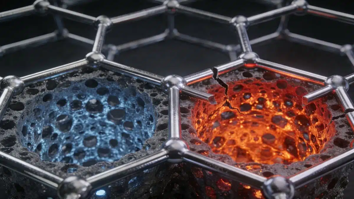
Maximizing of tantalum capacitor capacitance values within a fixed anode volume requires increasing specific surface area, which inherently reduces the characteristic interparticle neck size (X). At the same time, higher formation voltages increase dielectric thickness (d).

RelatedPosts

From DCL to SSC: Bridging Electrical Symptoms and Structural Indicators in Tantalum Capacitors

Using a Virtual Anode Thermal Model to Evaluate Miniaturization Risk in Tantalum Capacitors

Practical Value of Structural Diagnostics for Tantalum Capacitor Anodes

This work shows that these coupled effects lead to a critical increase in the structural parameter ψ = d/X, progressively constraining the conductive pathway of the metallic skeleton.

Using a physics-based thermal model /2/, it is demonstrated that this structural constriction results in a non-linear increase in local resistance and heat generation, ultimately triggering thermal instability and failure.

The analysis establishes that while capacitance is governed by surface area development, reliability is controlled by the structural integrity of the conductive network.

Introduction

In a tantalum capacitor design, the engineering objective is typically straightforward: maximize capacitance within a given case size and rated voltage.

This paradigm is often implicitly expressed as:

Process → Capacitance → Reliability

However, practical experience shows that capacitors with similar capacitance and ratings can exhibit significantly different leakage current (DCL) and breakdown voltage (BDV) behavior. Some devices remain stable, while others become failure-prone under stress.

This discrepancy indicates that capacitance alone does not fully describe the functional state of the anode. The origin of this inconsistency lies in porous materials.

While the manufacturing process defines nominal conditions (powder, pressing, sintering, formation), the resulting anode is a distribution of structural states, including variations in:

  • interparticle neck geometry
  • effective conductive cross-section
  • internal stress distribution

This leads to a fundamental principle of powder metallurgy:

Even for a fixed process, the resulting structure is a distribution of states: neck geometry, effective conductive cross‑section, internal stresses, and local defects vary throughout the anode. 

Process ≠ Structure

The tantalum anode is a porous sintered body. In such materials, we must distinguish between:

  • The structure: actual network of pores and metallic interparticle necks, their sizes, and distribution.
  • The process: powder grade, pressing, sintering, formation conditions.

Electrical behavior is governed not by process labels, but by the actual conductive network formed inside the anode.

Beyond the Classical Capacitance Model

The relation proposed by Lessner /1/ describes capacitance formation:

C⋅VrVol=(K⋅ε0)⋅AVol⋅Vrd​​with
C – capacitance,
Vr – rated voltage,
Vol – anode volume,
A/Vol – internal surface area per volume,
d – dielectric oxide thickness,
K – relative dielectric constant,
ε₀ – permittivity of free space.

This equation correctly defines the required surface area to achieve a given capacitance. However, it is blind to the structural conditions required for stable current transport.

In practice:

  • Increasing capacitance → requires higher A/Vol → leads to smaller neck size (X ↓)
  • Increasing voltage → requires thicker oxide → increases d

Thus, two opposing structural trends emerge simultaneously:

  • reduction of X (geometric thinning of the conductive skeleton)
  • increase of d (dielectric consumption of the conductive path)

The Double Constriction Effect

These two trends act in the same direction, creating a double constriction of the metallic skeleton:

  • geometric constriction (X ↓)
  • dielectric constriction (d ↑)

To quantify this interaction, a dimensionless structural parameter is introduced:

ψ=dX​where
d – dielectric oxide thickness,
X – characteristic interparticle neck size.

ψ measures how much of the neck has been “eaten” by oxide relative to its original size. As capacitance is increased (by higher A/Vol → smaller X) and rated voltage is raised (→ larger d), ψ grows and the conductive pathway becomes progressively more constrained. Thus, as ψ increases, the effective metallic cross‑section shrinks, causing:

  • Higher local electrical resistance in the neck.
  • Stronger localization of current.
  • Enhanced local heat generation.

ψ thus forms a bridge from geometrical design parameters (CV/g, formation voltage) to the physical mechanisms of thermal instability and failure.

Structural Meaning of ψ

Unlike Equation (1), which treats A/Vol and d independently, ψ links them through the physical geometry of the conductive channel.

As capacitance and voltage increase:

  • A/Vol ↑ → X ↓
  • d ↑
  • therefore ψ ↑

This leads to:

  • increased local resistance (Rₙₑcₖ)
  • current localization
  • enhanced local heat generation (Wₐ)

Thus, ψ acts as a bridge between design parameters and failure physics.

Experimental Evidence

Experimental data confirm that increasing capacitance leads to structural refinement:

  • Powder level: BET increases nonlinearly with CV/g
  • Sintered anodes: capacitance correlates with reduced neck size

This establishes a key structural relationship:

A/Vol↑→X↓

Capacitance growth is therefore achieved by thinning the conductive network, not by neutral structural scaling.

Physical Mechanism: Hot Spot Formation

The interparticle neck in the porous structure acts as a bottleneck for current transport. During anodization, part of its cross‑section is consumed by oxide growth. The effective metallic radius can be approximated as:

rmet≈X2−dAs ψ grows, the remaining metallic core shrinks. According to Joule’s law, local heat generation in the neck region is:

Wa=I2⋅Rneck≈I2⋅ρ⋅Lπ⋅(X/2−d)2​In first order, heat generation is inversely proportional to the square of the effective cross‑section. Even modest leakage currents can thus produce significant localized heating when ψ approaches critical values.

This leads to classical hot spot behavior:

  1. Local temperature rise increases dielectric conductivity.
  2. Current concentrates even more into the hot region.
  3. Additional heating accelerates degradation.
  4. Dielectric breakdown follows.

This leads to a positive feedback loop:

temperature rise → increased conductivity → current concentration → further heating → dielectric breakdown

This is the hot spot mechanism linking structure to failure.

Reliability Thresholds

Based on experimental observations and thermal modeling, three regimes can be defined:

Stable Region (ψ < 0.25)

  • uniform current distribution
  • effective heat dissipation
  • stable BDV and low DCL

Critical Region (ψ ≈ 0.25–0.30)

  • high thermal sensitivity
  • latent instability
  • DCL fluctuations under stress

Failure Region (ψ > 0.30)

  • severe current localization
  • overheating
  • high probability of dielectric breakdown

Design Implications

Although ψ is not directly specified in datasheets, its implications are clear:

  • highest CV in smallest case size → structurally aggressive design
  • combination of high capacitance + high voltage → increased ψ
  • margin in volume or derating → improved structural stability

Thus, conventional reliability practices (derating, thermal margin) gain a structural interpretation.

Thermal Model as a Design Tool

To translate structural effects into engineering parameters, a thermal model of the anode is used /2/.

The model links:

structure → Rneck → heat generation → thermal balance (Δ) → reliability

This enables:

  • early-stage design evaluation
  • overheating risk prediction
  • optimization of BET vs. X vs. formation voltage

Importantly, this approach allows designers to move from empirical trial-and-error to predictive structural design.

Conclusion

Equation (1) remains valid for describing capacitance formation, but it does not capture the structural limitations governing current transport. This work shows that capacitance optimization inherently drives:

  • reduction of interparticle neck size (X ↓)
  • increase of dielectric thickness (d ↑)

These effects act simultaneously, progressively constraining the conductive pathway of the metallic skeleton. The introduction of ψ = d/X provides a quantitative measure of this constraint and establishes a direct link between structure and failure physics. As ψ increases, local resistance and heat generation rise, leading to thermal instability and dielectric breakdown.

A key outcome of this work is the identification of structural reliability regimes, enabling early detection of overheating risk before electrical testing. The proposed approach transforms the classical capacitance relation into a structure-aware reliability framework, supported by thermal modeling and physical interpretation.

Final Statement

Reliability is not a purely electrical outcome — it is a structural property of the anode.

References

[1] P. Lessner, “Specific Capacitance and Formation Physics in Tantalum Capacitors”
https://www.philiplessner.com/blog/8

[2] V. Azbel, “Virtual Anode Thermal Model”
DOI: 10.5281/zenodo.19482660

Related

Source: Vladimir Azbel

Recent Posts

Samsung Electro-Mechanics MLCC capacitor solutions for high-voltage converter snubbing and GPU power delivery

Samsung MLCC Options for 1 MW AI Rack Power

18.9.2026
3
Frenetic planar ER transformer simulation for a 5 kW 800 V-to-50 V PSFB converter, showing low-profile core geometry and high-current planar winding arrangement

5 kW 800 V-to-50 V PSFB Transformer Design for Data Centers

18.9.2026
3
Exxelia PM film capacitor and passive-component technologies for BepiColombo space electronics

Exxelia Passive Components Support BepiColombo Mission

16.9.2026
21
TDK B43657 and B43658 ultra-compact snap-in aluminum electrolytic capacitors for 500 V DC power-supply and DC-link applications

TDK Extends Compact Snap-In Capacitors to 500 V for AI Servers

16.9.2026
30

Samsung MLCC Revenue Seen Above KRW 8T by 2027, Murata EOL Actions Reshape Supply

11.9.2026
73

LG Innotek Demonstrates FC-BGA Substrates With Embedded Silicon Capacitors for AI Power Delivery

10.9.2026
54

Emerging Capacitor Markets in Fusion Energy

10.9.2026
58
onsemi solid-state transformer concept for 800 V HVDC AI data center power conversion with SiC modules, DC-link capacitors and high-frequency magnetics

Solid-State Transformers for 800 V AI Data Centers: Passive Component Design Considerations

9.9.2026
123
TDK CN series 10 µF 100 V X7R soft-termination multilayer ceramic capacitor in 3225 EIA 1210 package

TDK Releases 100 V Soft-Termination X7R MLCCs 10 uF in 3225 Package

9.9.2026
37

Upcoming Events

Sep 29
16:00 - 17:00 CEST

Cybersecurity 2026

Sep 30
15:00 - 16:00 CEST

Positronic Space and Military Connectors

Oct 14
17:00 - 18:00 CEST

Live Demo! Discover KYOCERA AVX Antenna Integrator Studio (AIS)

View Calendar

Popular Posts

  • Buck Converter Design and Calculation

    0 shares
    Share 0 Tweet 0
  • LLC Resonant Converter Design and Calculation

    0 shares
    Share 0 Tweet 0
  • Boost Converter Design and Calculation

    0 shares
    Share 0 Tweet 0
  • Flyback Converter Design and Calculation

    0 shares
    Share 0 Tweet 0
  • Resistor Symbols

    0 shares
    Share 0 Tweet 0
  • Capacitor Charging and Discharging

    0 shares
    Share 0 Tweet 0
  • MLCC and Ceramic Capacitors

    0 shares
    Share 0 Tweet 0
  • Earthing Systems and IEC Classification Explained

    0 shares
    Share 0 Tweet 0
  • Audio Capacitors: Choosing Capacitors for Crossover Circuits

    0 shares
    Share 0 Tweet 0
  • Capacitor Symbols

    0 shares
    Share 0 Tweet 0

Newsletter Subscription


Passive Components Blog

© 2015–2026
All rights reserved

  • Home
  • Privacy Policy
  • EPCI Membership & Advertisement
  • About

No Result
View All Result
  • Home
  • Knowledge Blog
  • Dossiers
  • PCNS

© 2015–2026
All rights reserved