Samsung Electro-Mechanics has outlined MLCC placement options for power delivery in 1 MW-class AI server racks.
The Samsung release covers a high-voltage molded-frame ceramic capacitor for converter switching nodes, compact high-capacitance MLCCs for GPU core-power decoupling, and embedded-MLCC concepts intended to reduce interconnect inductance.
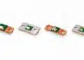
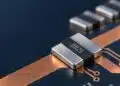
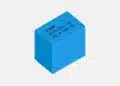
High-voltage switching support uses the CL55C543JI6MPN# molded-frame capacitor, a 2220-size C0G MLCC specified at 54 nF and 1,000 V DC.
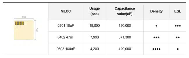
GPU core-power analysis compares 0201 10 µF, 0402 47 µF, and 0603 100 µF MLCC options, identified in the release as 03X106MS, 05X476MS, and 10X107MS.
The release focuses on the trade-off between capacitance density and equivalent series inductance (ESL), rather than treating nominal capacitance as the sole PDN selection criterion.
Samsung also presents horizontal embedded-MLCC mounting as a route to remove the need for plated through-holes at the capacitor connection, enabling a tighter power-delivery pitch.
Technical highlights
Parameter
Value
Notes
Series / construction
MFC, 2-stack
Molded Frame Capacitor
Part number
CL55C543JI6MPN#
High-voltage MLCC
Case size
2220 / 5750 metric
5.70 × 5.50 mm
Dielectric
C0G
Stable Class I ceramic
Rated voltage
1,000 V DC
Product documentation
Capacitance
54 nF
Nominal value
Temperature range
−55 °C to +125 °C
Product documentation
Qualification
AEC-Q200
Passive-component stress qualification
The current product documentation identifies CL55C543JI6MPN# as an automotive AEC-Q200-qualified, mass-production MFC part. The 1 MW rack release uses the same part as a high-voltage converter snubber example, but the underlying product documentation should govern component selection and qualification.
Proposal for Compact, High-Capacitance MLCCs for GPU Core Power
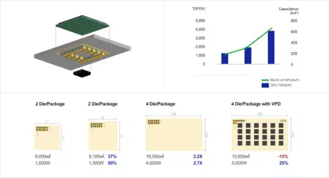
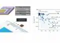
The MLCC capacitance density required for GPUs at least doubles each year. GPU power consumption is increasing much faster than the area of the GPU package allocated to core power. This means that more capacitors are required even as the available space remains limited.
When VPD(Vertical Power Delivery) is applied, the space available for MLCC placement becomes even more constrained. The following simulation results explore how capacitance density can be maximized.
“AI MLCC’s Law”: The MLCC capacitance required per GPU doubles every year.
MLCC option
Nominal capacitance
PDN role in release
0201, 03X106MS
10 µF
Lower-ESL local decoupling
0402, 05X476MS
47 µF
Capacitance / ESL compromise
0603, 10X107MS
100 µF
Higher capacitance density
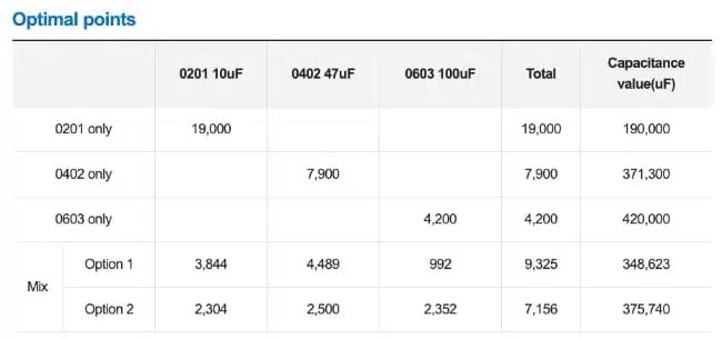
The release presents 0402 47 µF as the best single-size balance in its simulated 100 × 100 core-power area. It also shows that a mixed population of 0201, 0402, and 0603 MLCCs can improve impedance behaviour relative to a capacitance-maximised arrangement, provided the placement mix is optimised:
Typical applications
The 1,000 V DC rating, C0G dielectric and 54 nF capacitance support use of CL55C543JI6MPN# at high-frequency switching locations where a low-inductance capacitor path is required, including high-voltage DC-DC converter snubbers. Its voltage rating must still be checked against normal operating voltage, switching overshoot, surge events and fault transients.
The 0201, 0402 and 0603 high-capacitance MLCC examples target GPU core-power decoupling in dense power-distribution networks. Their cited function is to combine local capacitance with package-dependent ESL control as GPU current slew rate increases.
Samsung identifies embedded MLCC placement as a board-level option for dense GPU power delivery. The release does not provide public package drawings, electrical ratings, reliability reports, land-pattern guidance or production-status information for the embedded configuration, so those details should be requested before committing it to a PCB stack-up.
Application fit
Circuit position
Supported selection factor
Check before release
HV DC-DC snubber
1,000 V DC, 54 nF, C0G
Peak voltage and layout loop
GPU local decoupling
10 µF to 100 µF examples
DC-bias capacitance and PDN impedance
Dense core-power PDN
0201 to 0603 packages
Via pitch and mounting inductance
Embedded capacitor path
Horizontal electrode connection concept
PCB process and reliability evidence
For GPU power rails, MLCC DC bias and ageing capacitance loss remains a central selection issue. The release supplies nominal capacitance figures for its compact MLCC examples, but it does not publish voltage ratings, dielectric classes, DC-bias curves, impedance plots or thermal limits for the abbreviated 03X106MS, 05X476MS and 10X107MS designations.
The key system-level issue is impedance over frequency, not capacitance alone. Smaller packages can reduce ESL and extend decoupling effectiveness toward higher frequencies, while larger packages contribute more nominal bulk capacitance in the available PCB area.
Design-in notes for engineers
Use the 1,000 V DC rating of CL55C543JI6MPN# only after evaluating steady-state voltage, repetitive switching overshoot, abnormal conditions and applicable derating requirements.
Keep the snubber current loop short and wide; capacitor ESL is only one part of the loop inductance, alongside pads, copper geometry, vias and MOSFET package connections.
For high-CV GPU decoupling capacitors, validate effective capacitance under the intended DC bias, AC excitation, temperature and ageing state; nominal capacitance alone is not sufficient.
Build the PDN from impedance targets and placement constraints, then optimise the population of low-ESL and higher-capacitance MLCCs through measurement or verified simulation.
Verify that the selected package dimensions remain compatible with PTH pitch, breakout routing, assembly tolerances and rework requirements.
Treat horizontal embedded MLCC mounting as a PCB-and-component co-design task. This does not replace system-level validation of laminate compatibility, assembly flow, mechanical stress, inspection capability and long-term reliability.
This article is based on a Samsung Electro-Mechanics product-news release and official product documentation. Engineers should consult the current manufacturer datasheet, characteristic data and applicable qualification documentation before final qualification and design release.