
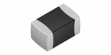






Samsung Electro‑Mechanics has introduced a new line‑up of ultra‑compact, ultra‑high‑capacitance MLCCs aimed at power stabilization in AI edge devices and wearables.
These Samsung Electro‑Mechanics‘s parts target designers who must combine higher AP/NPU power consumption with extremely limited PCB area and ultra‑slim mechanical envelopes.
Key features and benefits
- Ultra‑small footprints for dense layouts
The line‑up spans 01005 (0402 metric), 0201 (0603 metric) and 0402 (1005 metric) case sizes, enabling high capacitance in footprints traditionally reserved for decoupling rather than bulk storage. - High capacitance in miniature sizes
Offered values include 1 µF in 01005, 4.7 µF and 10 µF in 0201, and 22 µF in 0402, providing designers with bulk and mid‑range capacitance close to high‑current loads without large form‑factor capacitors. - Optimized for low‑voltage AI and comms rails
The voltage range from 2.5 V to 10 V fits typical subsystems such as NPUs/APs, RF and connectivity modules, sensors, and other low‑voltage ICs in edge devices. - Temperature characteristics suited to wearables
The line‑up combines X5R and X6S temperature characteristics, supporting operation over typical consumer and wearable temperature ranges while limiting capacitance drift versus temperature according to manufacturer datasheet. - Ultra‑thin profiles for slim devices
Maximum thickness values down to 0.25 mm in 01005 and 0.39 mm in 0201 help maintain tight z‑height budgets in smartwatches, AR/VR headsets, patches, and other ultra‑slim devices. - Reduction of part count and area
Higher capacitance per device in small footprints allows designers to reduce the number of parallel MLCCs and free routing area around APs, communication modules and sensors.
Market context and adoption trends
With on‑device AI moving computing from the cloud into local NPUs and application processors, instantaneous power demand and dynamic current transients have increased significantly in edge devices. This drives stronger requirements for local decoupling and bulk capacitance right at the IC pins to suppress ripple and noise on supply rails according to manufacturer datasheet.
At the same time, the available PCB area in wearables continues to shrink due to the integration of AI accelerators, multi‑standard communication modules (Bluetooth, Wi‑Fi, UWB), and diverse sensors. As more functions are squeezed into the same or smaller form factor, passive component footprints must scale down without sacrificing electrical performance.
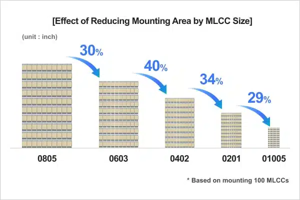
The new MLCC line‑up reflects an ongoing transition from traditional 0603–0402 sizes towards 0201 and even 01005 footprints for high‑capacitance parts. In parallel, the adoption of 22 µF and higher values in mainstream 0402 sizes for consumer devices is expected to expand as AI features propagate from premium into mid‑range and low‑end products.
Technical highlights
Flagship MLCC line‑up overview
| Part number | Size (inch / metric) | Capacitance | Rated voltage | TCC | Max thickness |
|---|---|---|---|---|---|
| CL02A105MQ2NQN# | 01005 / 0402 | 1 µF | 6.3 V DC | X5R | 0.25 mm |
| CL03A475MQ3CRN# | 0201 / 0603 | 4.7 µF | 6.3 V DC | X6S | 0.39 mm |
| CL03X106MS5C6W# | 0201 / 0603 | 10 µF | 2.5 V DC | X6S | 0.55 mm |
| CL05A226MP6NUN# | 0402 / 1005 | 22 µF | 10 V DC | X5R | 0.8 mm |
Temperature characteristics and implications
- X5R parts are specified for operation roughly within a mid‑range temperature span, with the capacitance staying within defined tolerances across that range according to manufacturer datasheet.
- X6S parts extend the usable temperature range and are suited for environments with slightly higher maximum temperatures, again with a guaranteed window for capacitance variation across the operating range as per datasheet.
In practice, X5R and X6S dielectrics are used where designers need reasonably stable capacitance under temperature, but can accept some variation compared with more stable dielectrics in exchange for higher volumetric efficiency.
Thickness and mechanical integration
Slim housings in wearables and healthcare patches impose strict limits on component height. Maximum thickness figures from 0.25 mm to 0.8 mm in this line‑up enable:
- Closer placement under shielding cans and mechanical frames.
- Easier stacking of PCBs or flex boards in multi‑layer device constructions.
- Reduced mechanical stress and clearance concerns around high‑profile components.
Typical applications
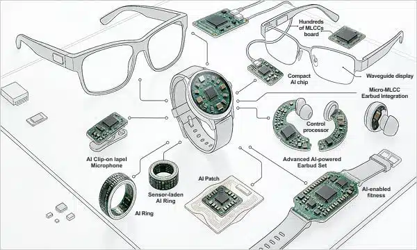
Wearables and edge AI devices often combine several rails and subsystems; these MLCCs are positioned to support:
- Power rails for APs and NPUs in smartwatches and AR/VR headsets.
- Local decoupling around AI accelerators mounted close to displays or sensor hubs.
- Bulk capacitance for connectivity modules integrating Bluetooth, Wi‑Fi and UWB.
- Sensor interface and analog front‑end rails in compact healthcare and fitness devices.
- Secondary rails in battery‑powered IoT endpoints where PCB area is highly constrained.
Beyond wearables, similar requirements appear in compact handheld devices, miniaturized medical electronics, and other form‑factor‑driven designs that integrate on‑device AI functions according to manufacturer press release.
Availability and part numbers
All four flagship MLCCs in the line‑up are currently listed as available for sampling:
- CL02A105MQ2NQN# – 1 µF, 6.3 V, X5R, 01005.
- CL03A475MQ3CRN# – 4.7 µF, 6.3 V, X6S, 0201, designated as low‑profile.
- CL03X106MS5C6W# – 10 µF, 2.5 V, X6S, 0201.
- CL05A226MP6NUN# – 22 µF, 10 V, X5R, 0402.
Sample requests and design support are available via the regional contact channels listed by Samsung Electro‑Mechanics for the USA, Europe, Southeast Asia, China, Japan and Korea.
Quick selection table by use case
| Application focus | Recommended size | Capacitance class | Example part |
|---|---|---|---|
| Extreme space constraint | 01005 | Around 1 µF | CL02A105MQ2NQN# |
| Ultra‑slim wearables | 0201 low‑profile | 4.7 µF class | CL03A475MQ3CRN# |
| Low‑voltage AI cores | 0201 | Around 10 µF | CL03X106MS5C6W# |
| Bulk rail stabilization | 0402 | Around 22 µF | CL05A226MP6NUN# |
Designers should verify exact electrical characteristics, tolerances and derating behavior in the respective datasheets rather than relying solely on summary values.
Design‑in notes for engineers
- Check effective capacitance under bias and temperature
High‑capacitance MLCCs in small case sizes exhibit voltage and temperature‑dependent capacitance; always refer to manufacturer curves for capacitance versus DC bias and temperature when sizing bulk and decoupling networks. - Account for ripple and transient current
On‑device AI workloads produce large dynamic current swings in APs and NPUs; ensure that the selected MLCCs, together with any additional bulk capacitors, keep supply rail ripple within IC limits under worst‑case transients and load steps. - Use proximity to minimize ESL and ESR
The benefit of high capacitance in 0201 and 01005 sizes is only fully realized when the devices are placed very close to the IC supply pins; short, wide routing and tight loops help reduce parasitic inductance and resistance. - Combine values for broadband decoupling
A mix of smaller capacitance values for high‑frequency decoupling and larger values (such as 10 µF and 22 µF) for lower‑frequency bulk stabilization often yields better impedance profiles than relying on a single capacitance per rail. - Respect mechanical and assembly constraints
Ultra‑thin MLCCs can be more sensitive to board flex and bending; follow the manufacturer guidelines for PCB layout, pad design, and mounting near board edges or cut‑outs to avoid cracking and reliability issues. - Validate reliability in target environment
Even for consumer wearables, consider life testing under representative thermal cycling, humidity and mechanical stress conditions, as small case sizes with high capacitance densities can be more demanding in terms of long‑term reliability. - Plan for product scaling
As AI features move to mid‑range and entry‑level devices, component platforms that offer pin‑compatible upgrades across capacitance values and case sizes simplify design reuse; review the broader MLCC portfolio around these flagship parts when planning future variants.
Source
This article is based on information provided in the official product news release published by Samsung Electro‑Mechanics and related MLCC product pages and documentation, with additional context and interpretation aimed at design engineers and component purchasers.