Passive Components Blog
No Result
View All Result
  • Home
  • NewsFilter
    • All
    • Aerospace & Defence
    • Antenna
    • Applications
    • Automotive
    • Capacitors
    • Circuit Protection Devices
    • electro-mechanical news
    • Filters
    • Fuses
    • Inductors
    • Industrial
    • Integrated Passives
    • inter-connect news
    • Market & Supply Chain
    • Market Insights
    • Medical
    • Modelling and Simulation
    • New Materials & Supply
    • New Technologies
    • Non-linear Passives
    • Oscillators
    • Passive Sensors News
    • Resistors
    • RF & Microwave
    • Telecommunication
    • Weekly Digest

    KYOCERA AVX Releases Compact High-Directivity Couplers

    Supercapacitors Emerge as a Promising Solution to AI-Induced Power Energy Spikes

    Wk 18 Electronics Supply Chain Digest

    YAGEO Releases High Current SMD Common Mode Choke With Shape Core Construction

    Murata and NIMS Built New Database of Dielectric Material Properties

    Tariffs Crush Sales Sentiment in April 2025 ECST Results

    High-Density PCB Assemblies For Space Applications

    Solid State Polymer Multilayer Capacitors For High Temperature Application

    Graphene-Based BOSC Bank Of Supercapacitor Cells

    Trending Tags

    • Ripple Current
    • RF
    • Leakage Current
    • Tantalum vs Ceramic
    • Snubber
    • Low ESR
    • Feedthrough
    • Derating
    • Dielectric Constant
    • New Products
    • Market Reports
  • VideoFilter
    • All
    • Antenna videos
    • Capacitor videos
    • Circuit Protection Video
    • Filter videos
    • Fuse videos
    • Inductor videos
    • Inter-Connect Video
    • Non-linear passives videos
    • Oscillator videos
    • Passive sensors videos
    • Resistor videos

    Coupled Inductors in Multiphase Boost Converters

    VPG Demonstrates Precision Resistor in Cryogenic Conditions

    Comparison Testing of Chip Resistor Technologies Under High Vibration

    EMC Challenges for High Speed Signal Immunity and Low EMI

    MOSFET Gate Drive Resistors Power Losses

    Modified Magnetic Reluctance Equivalent Circuit and its Implications

    Improving Common Mode Noise Reduction while Decreasing BOM

    Die and Wire PCB Bonding Explained

    Rogowski Coil Current Sensor Explained

    Trending Tags

    • Capacitors explained
    • Inductors explained
    • Resistors explained
    • Filters explained
    • Application Video Guidelines
    • EMC
    • New Products
    • Ripple Current
    • Simulation
    • Tantalum vs Ceramic
  • Knowledge Blog
  • Suppliers
    • Who is Who
  • Events
No Result
View All Result
Passive Components Blog
No Result
View All Result

IMEC Charts Semiconductors Roadmap Path Beyond 1nm

8.8.2022
Reading Time: 2 mins read
A A
source: IMEC

source: IMEC

Belgian research lab IMEC has charted the roadmap path to semiconductor process technology and chip design below 1nm down to the A2 two angstrom generation.

At the recent Imec Technology Forum in San Francisco, Imec CEO Luc Van den hove laid out a 20 year roadmap for the evolution if semiconductor technology.

RelatedPosts

KYOCERA AVX Releases Compact High-Directivity Couplers

Supercapacitors Emerge as a Promising Solution to AI-Induced Power Energy Spikes

Wk 18 Electronics Supply Chain Digest

“We are convinced that Moore’s Law will not stop, but there will be many approaches that will all contribute,” said Luc van den Hove, CEO of IMEC

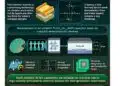
Future transistor architectures may include GAA devices built from a stack of nano sheets, den hove described several including a gate-all-around device built up of a stack of nanosheets and the forksheet device in which the N and the P channel transistors are moved closer together and the CFET where N and P transistors are stacked on top of each other.

“This forksheet device, we see as an extension of the standard nano sheet concept, and we believe it will be introduced around the equivalent of the one nanometer generation,” said Van den hove.

“It’s clear that you can realize another very important step in cell size shrinking, but obviously at the expense of much more complex contacting schemes to contact the source and drain areas. But we believe that we have developed integration schemes that would enable such transistors by optimizing the epi processes, patterning processes, and leveraging very sophisticated deposition processes to enable the contacting structures,” said Van den hove.

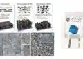
Possible ways ahead are reducing the thickness of the silicon channels to reduce channel length by replacing the silicon with 2D materials — atomically flat mono layers — such as tungsten or molybdenum sulfides or selenides.

“We’ve recently demonstrated the first versions of devices fabricated using 300 millimeter equipment,” he said.

But we also need to improve the performance of the interconnect. One interesting option is to move the power delivery to the back of the wafer. This leaves more design flexibility for the interconnect on the front side. “All of this results in scaling for the next fifteen to twenty years,” he said. 

A combination of continued dimensional scaling, new transistor architectures, new materials introduction, combined with innovative interconnect architectures (buried power rails) will be the secret to success.

“We believe that we can propose a roadmap for the next eight to 10 generations — with an introductory pace of two to two-and-a-half year cadence — would bring us a roadmap for the next 20 years,”  said Van den hove.

“We need to take into account the sustainability of manufacturing of these devices, the electricity use, the water, the chemicals. In optimising these processes it is not enough to look at the performance, power and area but we have to take into account the environmental aspects of these technologies.

Related

Source: IMEC

Recent Posts

Murata and NIMS Built New Database of Dielectric Material Properties

5.5.2025
41

3D Printing of Passive Components from Manufacturer Perspective

26.4.2025
43

Hybrid Electrochemical Electrolytic Capacitor Provides High Frequency and High Capacitance Performance

25.4.2025
47

Supercapacitor Separator with High Ionic Conductivity Enables Line-Filter Applications at High Power

21.3.2025
46

Interlacing Strain Engineering Boost Energy Density of MLCCs

12.2.2025
83

Researchers Developed BaTiO3 based MLCC Material with High Energy Density at High Temperature Range

21.1.2025
104
A film a few atoms thick of non-crystalline niobium phosphide conducts better through the surface to make the material, as a whole, a better conductor. | Il-Kwon Oh / Asir Khan

Researchers Developed High Conductive Nanowires

20.1.2025
47

CNF-MIM Capacitors Benefits vs Deep Trench Capacitors

9.1.2025
111

Researchers Optimize MLCC Dielectric to Boost its Energy Density up to 20J per cc

6.1.2025
73

Researchers Increase Cell Voltage of Aqueous Supercapacitors by Electrode Surface Adjustments

31.12.2024
65

Upcoming Events

May 14
11:00 - 12:00 CEST

Reliable RIGID.flex PCBs for Critical Applications – Made in Europe

May 28
16:00 - 17:00 CEST

Power Over Data Line

View Calendar

Popular Posts

  • Buck Converter Design and Calculation

    0 shares
    Share 0 Tweet 0
  • Boost Converter Design and Calculation

    0 shares
    Share 0 Tweet 0
  • Flyback Converter Design and Calculation

    0 shares
    Share 0 Tweet 0
  • Tariffs Crush Sales Sentiment in April 2025 ECST Results

    0 shares
    Share 0 Tweet 0
  • What is a Dielectric Constant and DF of Plastic Materials?

    4 shares
    Share 4 Tweet 0
  • LLC Resonant Converter Design and Calculation

    0 shares
    Share 0 Tweet 0
  • Ripple Current and its Effects on the Performance of Capacitors

    3 shares
    Share 3 Tweet 0
  • Dual Active Bridge (DAB) Topology Explained

    0 shares
    Share 0 Tweet 0
  • SEPIC Converter Design and Calculation

    0 shares
    Share 0 Tweet 0
  • Flying Capacitors Explained

    0 shares
    Share 0 Tweet 0

Newsletter Subscription


Passive Components Blog

© EPCI - Leading Passive Components Educational and Information Site

  • Home
  • Privacy Policy
  • EPCI Membership & Advertisement
  • About

No Result
View All Result
  • Home
  • Knowledge Blog
  • Premium Suppliers

© EPCI - Leading Passive Components Educational and Information Site

This website uses cookies. By continuing to use this website you are giving consent to cookies being used. Visit our Privacy and Cookie Policy.
Go to mobile version