
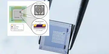






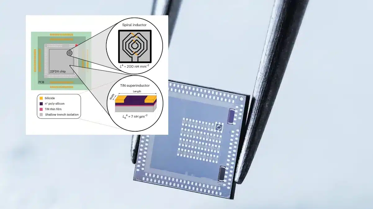
A team spanning Quantum Motion, the London Centre for Nanotechnology, CIC nanoGUNE, Imperial College London and the University of Cambridge has demonstrated TiN superinductors using a thin film already present in a commercial silicon manufacturing process.
Published in Nature Electronics on 4 November 2026, the peer-reviewed study combines these inductors with a silicon single-electron transistor to demonstrate a compact cryogenic charge-sensing circuit.
Key takeaways
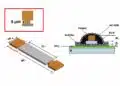
- A TiN strip measuring 0.36 × 50 µm provides estimated inductances of 149 nH or 131 nH, depending on the resistor-stack variant, in an active strip area of 18 µm².
- The two variants have superconducting transition temperatures of 0.75 K and 1.1 K. These are sub-kelvin devices, not replacements for room-temperature RF inductors.
- Reported inductance densities are approximately 8 and 7 nH/µm², respectively, with internal resonator quality factors around 50.
- The integrated charge sensor achieves a power signal-to-noise ratio of 4,500 at a 4 ns integration time. Its reported 1 ± 0.3 ps minimum integration time is an extrapolated sensitivity metric—not a demonstrated picosecond measurement.
Background
Conventional integrated inductors obtain most of their inductance from magnetic flux associated with a conductor’s geometry. Shrinking a spiral therefore tends to reduce its inductance, leaving inductors disproportionately large relative to transistors.
Kinetic inductance offers a different route. It arises from the inertia of charge carriers: changing the current requires changing their velocity. In a sufficiently thin superconducting film, this contribution can dominate, allowing a narrow strip to provide substantial inductance without a large spiral.
The principle is not new. The paper places its work alongside Josephson-junction-array superinductors, superconducting nanowires and earlier high-impedance TiN microwave circuits. Its distinctive contribution is implementation in GlobalFoundries’ commercial 22FDX fully depleted silicon-on-insulator process, rather than a dedicated superconducting fabrication flow.
Previous coverage of kinetic-inductance-based miniaturization describes a different materials route using intercalated graphene. The important distinction here is superconducting operation at deep-cryogenic temperatures.
A superinductor is defined by impedance, not simply by having a large inductance. The relevant intrinsic impedance must exceed the superconducting resistance quantum, approximately 6.45 kΩ. Parasitic capacitance therefore matters alongside inductance.
What the researchers found
The devices exploit TiN within two existing poly-resistor structures. Type A has compensated polysilicon above the TiN; type B uses n⁺-doped polysilicon. This is a thin-film integrated structure, not a ferrite-core or wound component.
Four-terminal current–voltage measurements characterize strips with widths from 0.36 to 3.6 µm and lengths from 0.36 to 50 µm. An on-chip multiplexer addresses the characterization array. Static dissipation from its supply circuitry establishes an on-chip temperature floor around 350 mK, illustrating why refrigerator temperature and actual device temperature must be distinguished.
Separate resonator measurements extract inductance from the measured resonance and modeled capacitance.
| Parameter | Type A | Type B | Conditions and interpretation |
|---|---|---|---|
| Superconducting transition temperature | 0.75 K | 1.1 K | Extracted from resistance–temperature measurements |
| Estimated strip inductance | 149 nH | 131 nH | Superconducting resonator extraction; strip geometry 0.36 × 50 µm |
| Sheet kinetic inductance | 1.07 nH/square | 0.94 nH/square | Calculated from extracted inductance and strip aspect ratio |
| Active-strip inductance density | Approximately 8 nH/µm² | Approximately 7 nH/µm² | Inductance divided by 18 µm² strip area; excludes complete circuit overhead |
The paper reports internal quality factors around 50 for both variants. Its temperature-dependent inductance plot includes one type-A device and three type-B devices: useful evidence of device operation, but not a wafer-level process distribution.
Inductance increases with temperature, in-plane magnetic field and applied current. Measurements show superconducting resilience to in-plane fields up to 2 T, while also showing that magnetic field changes the inductance. Field tolerance should therefore not be confused with parameter stability.
For the application demonstration, the inductor shares a chip with metal–oxide–metal capacitors and a silicon transistor configured as a single-electron transistor. Changes in transistor resistance alter the reflected RF signal.
At incident powers above approximately −82 dBm, nonlinear inductance provides an additional sensing mechanism. A resistance change modifies resonator dissipation, which changes its internal excitation and shifts the current-dependent inductance. The resulting frequency shift supplements ordinary amplitude-based detection.
In this regime, the fitted minimum integration time scales approximately as , compared with at lower powers. Increasing excitation eventually drives the film normal and eliminates the resonance.
Why it matters for passive components
The immediate relevance is to integrated cryogenic inductors and LC matching networks—not mainstream power magnetics.
The reported strip inductance density exceeds the paper’s conventional CMOS spiral reference by more than four orders of magnitude. However, this comparison concerns the inductive element’s active area. Capacitors, routing, transistor structures, bond pads and readout electronics still occupy space.
The second consequence is reduced separation between the inductor and its load. The demonstrated circuit places the transistor approximately 1 µm from the TiN structure, limiting interconnect overhead. Its modeled inductor parasitic capacitance is approximately 6.3 fF.
A third consequence is that nonlinearity becomes useful rather than merely an error source. Current-dependent inductance can enhance sensing, but it also creates drive-dependent resonance and limits usable excitation power. A designer needs a nonlinear model, not just a nominal inductance value.
The qualification boundary is equally important. The paper calculates an intrinsic impedance around 11.5 kΩ using its maximum measured inductance of 807 nH and the small parasitic capacitance. That is not the impedance of every operating point, nor the input impedance of the complete loaded resonator.
The authors identify potential applications in parametric amplifiers, kinetic-inductance detectors and resonator arrays. These remain development directions; the demonstrated application is RF charge sensing.
From lab to component
An editorial maturity estimate is TRL 4: an integrated device and sensing function validated in a laboratory. Fabrication in a commercial process materially strengthens the manufacturing case, but does not establish a qualified foundry component.
Several limitations remain.
First, operation requires temperatures well below the transition temperature. The higher-transition-temperature variant still does not support operation at a conventional liquid-helium temperature.
Second, an internal quality factor around 50 is finite and application-dependent. Superconductivity does not make the complete resonator lossless, and the reported result alone does not establish suitability for demanding coherent quantum circuits.
Third, parasitic capacitance is taken from a conventional-temperature foundry model and assumed not to change substantially in the cryogenic superconducting regime. Direct verification would improve confidence in extracted inductance and impedance.
Fourth, manufacturing readiness needs distributions across wafers and lots, contact-resistance control, thermal-cycle repeatability and stable nonlinear parameters. The accessible paper does not establish long-term qualification or a production yield specification.
For sourcing engineers, availability is consequently tied to a specific integrated process implementation, not a catalog inductor. MLCC co-firing and base-metal capacitor electrodes are not the relevant compatibility questions here; process-stack access, foundry-supported models and cryogenic characterization are.
What engineers should watch
- Wafer- and lot-level distributions of transition temperature, sheet inductance, quality factor and switching current.
- Measured cryogenic parasitic capacitance and contact loss, replacing assumptions inherited from warmer-temperature models.
- Frequency and inductance stability versus actual chip temperature, magnetic-field orientation and combined DC/RF excitation.
- Demonstrated transient charge or spin readout, including resonator settling and fidelity—not only extrapolated sensitivity.
- Multiplexed-array performance, including frequency collisions, crosstalk, routing area and total cryogenic heat load.
- Foundry-supported nonlinear models, design rules and repeatable thermal-cycle qualification.
Summary
The study demonstrates compact superconducting inductors using TiN already present in a commercial CMOS process, then uses their nonlinear response to improve integrated charge sensing. It establishes a credible laboratory route to dense cryogenic inductance, not a qualified commercial passive component.
The designer’s takeaway is that inductance density alone is insufficient: temperature, parasitic capacitance, loss and drive-dependent behavior determine whether the compact element is useful in a real circuit.
Source
This article is based on the peer-reviewed paper published in Nature Electronics and the accompanying CIC nanoGUNE institutional news release. The publisher identifies the paper as open access, but the exact reuse license could not be verified from the retrieved material. These are research results rather than qualified commercial components; design decisions should await manufacturer-supported data and appropriate qualification.
References
- Thomas H. Swift, Alberto Gomez-Saiz, Fabio Olivieri, Gorka Aizpurua-Iraola, Manuel Suárez-Rodríguez, James Kirkman, Grayson M. Noah, Mathieu de Kruijf, Felix-Ekkehard von Horstig, John J. L. Morton and M. Fernando Gonzalez-Zalba, “A nonlinear superinductor in a deep-submicrometre integrated circuit,” Nature Electronics, published online 4 November 2026, https://doi.org/10.1038/s41928-026-01728-8. Publisher-designated open access; exact license and final volume/page assignment not verified. Full article text and Methods accessed on the publisher’s HTML page.
- CIC nanoGUNE, “A new superinductor created within a silicon integrated circuit,” 4 November 2026, https://www.nanogune.eu/en/research/quantum-hardware/news/new-superinductor-created-within-silicon-integrated-circuit. Institutional news release; explicit image-reuse license not identified.