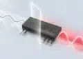

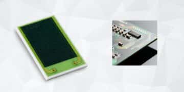








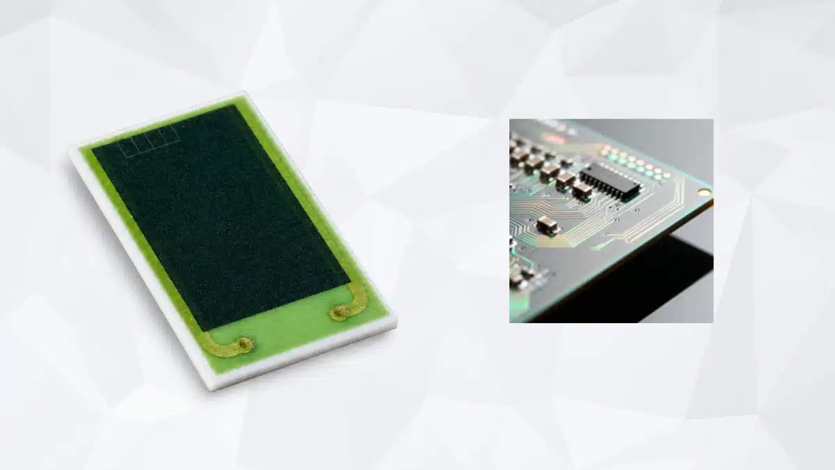
Miba Resistors has introduced the SC-55 series of SMD thick-film power resistors with a 55 W rating and a TO-263-compatible footprint.
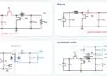
The thick-film power resistors series covers resistance values from 500 mΩ to 1 kΩ and targets power-conversion circuits, including pre-charge, snubber, bleeder and gate-resistor positions.
Key features and benefits
- TO-263-compatible footprint supports integration into board layouts using D2PAK power resistors.
- Resistance values extend from 500 mΩ to 1 kΩ, with higher values available on request.
- Resistance tolerances range from ±0.5% to ±10%.
- Operating temperature spans −55 °C to +175 °C.
- Component weight is below 0.4 g.
- Internal silver-paste-filled vias connect the resistive element to the solder pads, rather than routing the electrical connections around the component edges.
Technical highlights
Electrical and thermal selection parameters
The 55 W power rating makes thermal design a central selection consideration. Resistance, initial tolerance and temperature coefficient must also be considered together: the tolerance defines the initial resistance window, while the temperature coefficient governs resistance variation as the component temperature changes.
| Parameter | Value | Conditions |
|---|---|---|
| Rated power | 55 W | Thermal design dependent |
| Resistance range | 500 mΩ–1 kΩ | Higher values on request |
| Resistance tolerance | ±0.5% to ±10% | Other tolerances on request |
| Resistance measurement temperature | +25 °C ±3 °C | Resistance and tolerance |
| Operating temperature | −55 °C to +175 °C | — |
| Footprint compatibility | TO-263 / D2PAK | Surface mount |
| Weight | <0.4 g | — |
The temperature coefficient of resistance depends on the selected resistance value.
| Resistance range | Temperature coefficient |
|---|---|
| <2 Ω | ±500 ppm/°C |
| 2 Ω–10 Ω | ±250 ppm/°C |
| >10 Ω | ±100 ppm/°C |
The lower-resistance versions therefore require a different temperature-error allowance from versions above 10 Ω. Initial tolerance and temperature-dependent resistance change should remain separate entries in the circuit’s error budget.
Via-connected solder pads
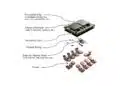
The SC-55 uses an internal connection path from the resistive element to the PCB-facing solder pads. Conductive paste on the top layer contacts the resistor paste, while silver paste fills a pre-drilled hole leading to the solder pad.
This construction places the electrical connection through the component rather than around its edge. Pad geometry, solder distribution and the assembled joint are consequently relevant to layout and process development. The connection arrangement is compatible with automated SMD assembly.
Typical applications
The SC-55 supports several circuit positions in power electronics:
- Pre-charge circuits.
- Bleeder and discharge paths.
- Snubber networks.
- Gate-resistor positions.
- Filter circuits.
Target systems include motor drives, power supplies, DC/DC converters, automotive electronics, power-generation equipment, energy-storage devices and medical equipment.
Application fit
Pre-charge and bleeder circuits draw on the series’ resistance range and power-handling capability. Selection should distinguish a charging pulse from sustained dissipation: a resistor that meets the continuous operating requirement must also accommodate the actual pulse duty.
Snubber and gate-resistor positions place emphasis on switching behaviour and pulse loading. Resistance value, repetitive heating and the assembled connection geometry should be assessed together rather than selecting from nominal wattage alone.
In motor drives, converters and storage equipment, the −55 °C to +175 °C operating range is relevant to the component’s thermal environment. It does not make the full rated power available throughout that temperature span; allowable dissipation must be matched to the installed thermal conditions.
Design-in notes for engineers
- Select resistance and initial tolerance from the circuit requirement, then include the applicable resistance-dependent temperature coefficient.
- Establish the heat-removal path before fixing the continuous dissipation target. Treat the 55 W rating as part of the thermal design, not as a board-independent dissipation allowance.
- Assess pulse duration, repetition rate and average dissipation together for pre-charge and snubber duties.
- Use TO-263 compatibility as the starting point for a D2PAK layout migration. Check pad alignment, solder distribution and the assembled thermal path before production release.
- Validate final selection under the actual electrical, thermal and assembly conditions.
Further reading
Source
This article is based on the Miba Resistors product announcement and official product documentation. Engineers should refer to the current manufacturer datasheet for final design and qualification.