






SMPS topology selection starts with the isolation requirement, required output power and complete input-to-output voltage range.
This guide helps design engineers compare buck, boost, buck-boost, isolated buck, flyback, forward and LLC architectures before selecting magnetics, switching devices and control circuitry.
Key Takeaways
A suitable topology must satisfy the complete operating envelope, not simply produce the correct output under nominal bench conditions.
- Define why isolation is required. Ground separation and personnel protection impose different requirements, and galvanic isolation alone does not establish safety compliance.
- Choose buck when the input remains sufficiently above the output, boost when it remains below the output, and buck-boost when it crosses the output voltage.
- Use isolated-topology power ranges to shortlist candidates, not as absolute operating limits or guaranteed efficiency rankings.
- Validate light-load behaviour, battery sag, load transients and input/output crossover before committing to the architecture.
- For isolated buck converters, check secondary regulation and cross-loading. Turns ratio, nominal inductance and package size do not establish magnetic-component interchangeability.
Why topology selection matters
Familiarity can reduce design time, but repeatedly adapting the same converter architecture can introduce unnecessary component stress, cost or efficiency compromises. A flyback that worked well in a low-power product is not automatically the best starting point for a substantially higher-power supply.
A topology describes the arrangement of magnetics, switching devices and other components and, more importantly, how that arrangement transfers energy. Two converters can use entirely different component part numbers while remaining the same topology. Würth Elektronik’s introductory SMPS podcast uses this distinction to build a practical architecture-selection framework. [1]
The energy-transfer mechanism influences:
- The number and function of magnetic components.
- Switching-device stress and switching losses.
- Circuit complexity and component count.
- Output-regulation behaviour.
- Control-loop requirements.
- The source and load conditions under which the converter can maintain its output.
The objective is not to learn every available topology. It is to recognise when a familiar architecture remains appropriate and when an alternative deserves investigation.
A practical SMPS topology selection decision tree
A useful selection sequence combines the broad architectural questions from Part 1 of Würth Elektronik’s podcast series with the operating-range checks developed in Part 2. Establish these requirements before detailed component calculations begin. [1, 2]
- Establish whether galvanic isolation is required and define its function.
- Define the required output power, including the loading of each output.
- Identify the source type and actual input-voltage range presented to the switching stage.
- Determine whether input voltage remains above, remains below or crosses the required output voltage.
- Check regulation, light-load operation, transient response and any secondary-output requirements.
Figure 1 arranges these questions as a decision tree. The isolation decision splits the field first; the non-isolated branch then follows the input-to-output voltage relationship, while the isolated branch follows power level, regulation need and component stress.
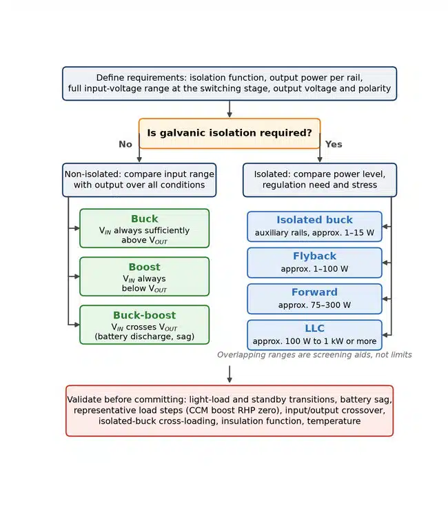
These decisions narrow the field before committing to a controller, transformer or inductor. For supporting circuit-level background, the guide to DC-DC converter characteristics and basic formulas provides the next step.
Isolation: define the function before choosing the circuit
Galvanic isolation separates input and output circuits without a direct conductive connection. In the isolated SMPS architectures considered here, power crosses that barrier through a transformer or coupled magnetic component. [1, 2]
Where the application does not require isolation, buck and boost architectures offer relatively simple, scalable conversion paths. Avoiding an isolation barrier can also avoid its transformer, barrier-related feedback arrangements and insulation-spacing requirements. These are architectural opportunities, not guarantees that every non-isolated implementation will be smaller or more efficient than every isolated alternative.
Why isolation may be necessary
Isolation requirements can arise from several different system needs:
- Protecting users from hazardous voltages.
- Separating ground references in sensors and measurement equipment.
- Addressing interference associated with nearby equipment, such as motor drives.
- Supporting fault separation in systems such as telecom racks.
These purposes are not interchangeable. A barrier used to separate signal references does not automatically provide the insulation required for personnel protection. Likewise, the need for isolation cannot be decided solely from whether the equipment is battery-powered or mains-powered; the complete system and accessible circuits matter. [1, 2]
Isolation does not automatically solve EMI
A transformer can provide galvanic separation while also becoming a source of electromagnetic interference if its implementation is unsuitable. Isolation should therefore be selected for a defined system function, not treated as a universal noise remedy. [1]
Evaluate the magnetic component, switching-current paths, circuit implementation and PCB layout together. For personnel protection, transformer insulation and PCB creepage and clearance must satisfy the requirements applicable to the end equipment. Neither the topology name nor the nominal output voltage establishes the required insulation rating. [2, 5]
Power level: use topology ranges as screening guidance
Power level becomes particularly useful when comparing isolated architectures. Table 1 preserves the approximate ranges discussed in the introductory podcast, and Figure 2 plots them on a logarithmic power axis; they overlap deliberately and are not hard operating limits. [1]
| Isolated topology | Approximate power range discussed | Main selection consideration |
|---|---|---|
| Isolated buck | 1–15 W | Simple auxiliary-power architecture; the primary non-isolated output may be unused by an external load. |
| Flyback | 1–100 W | Low circuit complexity and cost, with increasing stress and loss considerations as power rises. |
| Forward | 75–300 W | Additional circuitry may be justified by the required stress distribution and efficiency. |
| LLC | 100 W to 1,000 W or more | Resonant operation enables soft switching within the designed operating region. |
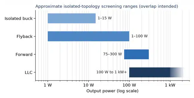
The practical lesson is not to replace one fixed rule with another. Increasing power should trigger a fresh comparison of architectures, including their semiconductor stresses, magnetic losses, thermal requirements and control behaviour.
Non-isolated buck and boost conversion can also scale into approximately kilowatt-class applications where system requirements permit, including some data-centre, motor-drive and telecom systems. That observation does not establish that a particular controller, magnetic component or single-phase implementation is suitable at that power. [1]
Why flyback remains a common starting point
Flyback conversion combines a relatively simple circuit with a well-established design approach. Applications include consumer charging equipment, industrial supplies and Power over Ethernet devices such as cameras and wireless access points. [1]
Its magnetic component stores energy for subsequent delivery to the output. This distinguishes its operation from a forward converter, which transfers energy to the secondary during the switch-on interval. Figure 3 shows the difference in the winding polarity and secondary circuit of the two basic single-switch forms.
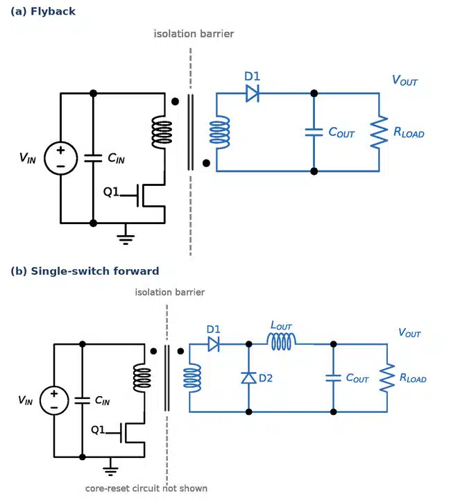
The introductory comparison uses a basic single-switch flyback to illustrate the relationship between simplicity and component stress. It should not be read as a description of every flyback variant or as evidence that all flybacks share the same practical power ceiling. [1]
When forward or LLC deserves investigation
As power increases, the simplicity of a basic flyback can become less attractive if its stresses and losses conflict with the requirements. A forward converter offers a different energy-transfer arrangement: during switch-on time, energy transfers through the transformer towards the output; during switch-off time, the output inductor continues supplying the load through the freewheeling path shown in Figure 3(b). [1]
The additional circuitry can be justified where efficiency and stress management matter more than minimum component count. Applications discussed in the introductory comparison include cordless-tool battery chargers and higher-power industrial supplies. The actual switch stress still depends on the selected implementation and reset arrangement; it is not determined by the word “forward” alone. [1]
LLC moves the comparison towards resonant conversion and soft switching. These operating principles can reduce switching losses, but the required input range, output range and load range must remain compatible with the design. High efficiency should not be inferred from the topology name without checking the intended operating conditions. [1]
Push-pull is another candidate where input voltage is relatively low. Its detailed magnetic and control design lies beyond this introductory comparison. [1]
AC/DC or DC/DC: examine the voltage presented to the power stage
The source label alone does not determine the topology. The architectures discussed here process DC at their underlying conversion stage, so an AC-input implementation must also provide the necessary rectification arrangement. [1]
The subsequent architecture must accommodate the resulting input-voltage range, required conversion ratio and isolation requirements. The podcast illustrates offline conversion using 120 V or 240 V AC sources and low-voltage outputs such as 12 V or 5 V. These are application examples, not a complete mains specification or safety-design prescription. [1]
The useful questions are:
- What minimum and maximum voltage reach the switching stage?
- How far must that voltage be stepped up or down?
- What isolation function does the complete system require?
An architecture that suits a low-voltage DC source should not be carried into an offline application without revisiting those conditions. The rectification stage and any preceding conversion stage belong in the system-level operating specification.
Non-isolated selection: follow the complete voltage range
Once isolation is unnecessary, the relationship between input and output becomes the central selection criterion. Table 2 summarises the first screening decision; controller limits and component stresses still require separate validation. [2]
| Topology | Required voltage relationship | Main validation concern |
|---|---|---|
| Buck | Input remains sufficiently above the required output. | Minimum input voltage, attainable duty cycle and light-load behaviour. |
| Boost | Input remains below the required output. | Conversion ratio, current stress, transient response and control-bandwidth constraints. |
| Buck-boost | Input can move above and below the required output. | Output polarity and operation across the input/output crossover region. |
Figure 4 applies Table 2 to one illustrative source. The same single-cell lithium-ion supply can require a buck, a boost or a buck-boost, depending on which rail it must supply and on how far the cell voltage falls with discharge and load.
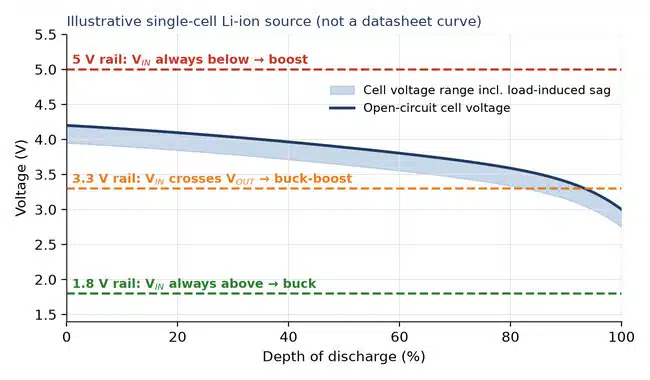
An isolated buck belongs to a separate branch. It derives an isolated auxiliary output from a buck-based stage rather than providing another non-isolated voltage-conversion relationship.
Current paths influence capacitor and layout requirements
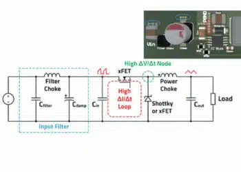
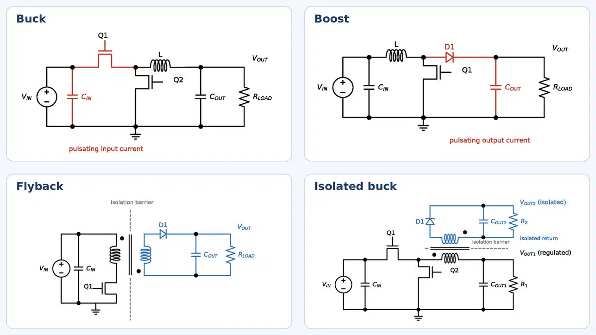
The voltage relationship is not the only difference between topologies. A conventional buck draws a pulsating switching current at its input, whereas a conventional boost delivers a pulsating rectifier current to its output. Consequently, the input and output capacitors do not perform identical ripple-current duties in the two circuits. Figure 5 highlights the pulsating branches. [3, 5]
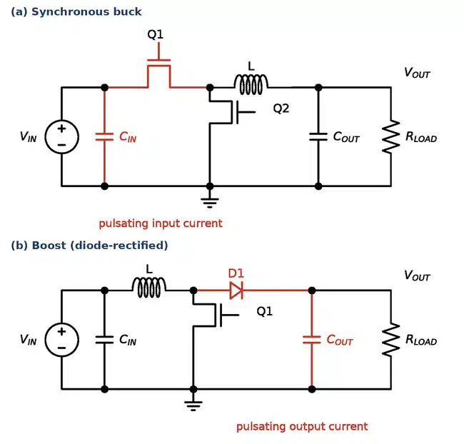
Identify the switching-current loops before selecting capacitors or finalising the layout. Compare capacitor ripple-current capability and impedance with the actual circuit waveforms, and keep high-frequency current paths compact. Do not assume that a capacitor arrangement proven in a buck transfers unchanged to a boost or buck-boost design. [3, 5]
Buck converters: step-down conversion with light-load checks
A buck is a natural starting point when the input remains sufficiently above the required output throughout the specified operating range. Examples include reducing a 12 V or 48 V distribution bus to 5 V, 3.3 V or lower-voltage rails for logic and sensors. [2]
The important qualification is “throughout the operating range”. A nominal-voltage comparison does not establish that the converter will remain regulated under every required source and load condition. The buck converter design and calculation guide develops the component-sizing stage after this architectural choice.
CCM and DCM affect the operating model
In conventional positive-current continuous conduction mode, or CCM, the inductor current remains above zero throughout the switching cycle. In discontinuous conduction mode, or DCM, current reaches zero and remains there for part of the cycle. Entering DCM changes the relationship between duty cycle, load and output voltage. [2, 3]
A synchronous buck does not necessarily enter DCM when the load falls. A forced continuous operating mode can allow the inductor current to reverse instead of stopping at zero, while other modes suppress reverse current and may skip switching pulses. Figure 6 compares the three inductor-current shapes. Check the controller’s selected operating mode rather than assuming that all light-load operation follows the same model. [6]
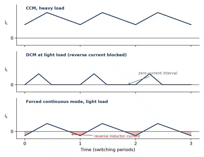
Dynamic behaviour established at substantial load cannot automatically be assumed to remain unchanged in standby. Test the actual controller and configuration at light load and during transitions back to active operation, including the resulting output ripple and recovery behaviour.
Battery sag can invalidate a buck-only choice
A battery’s nominal voltage may sit comfortably above the target rail while its voltage near the end of discharge, or under load, does not. Once the input falls below the required output, a buck cannot supply the missing step-up function. Figure 4 shows this case for the 3.3 V rail. [2]
A design can therefore pass early tests with a fresh battery or laboratory supply and lose regulation later. The correct topology follows the specified battery operating range, including load-induced sag, rather than nominal voltage alone.
Boost converters: step-up conversion with a transient constraint
A boost converter suits applications in which the input remains below the required output. Its conversion mechanism also introduces current and transient-response considerations that must be checked independently of the nominal voltage ratio. [2, 3]
For an ideal boost power stage in CCM, the output voltage VO follows from the input voltage VI and the duty cycle D, the fraction of the switching period during which the switch conducts, as given by Eq. (1). [3]
Typical application examples include:
- Raising a single-cell battery voltage of approximately 3–4 V to 5 V.
- Driving LED strings requiring more voltage than the source provides.
- Providing the boost function in many offline power-factor-correction front ends.
These examples establish application fit, not component values or guaranteed performance. In particular, the inductor and switching devices must carry the current required by the conversion process; their ratings cannot be selected from output current alone. [2, 3]
Understanding the right-half-plane zero
For a conventional boost power stage operating in CCM, the duty-cycle-to-output-voltage transfer function contains a right-half-plane zero. This qualification matters: the corresponding low-frequency DCM model does not have the same right-half-plane-zero behaviour. [3]
In the diode-rectified CCM arrangement, energy reaches the output through the diode during the switch-off interval. Increasing duty cycle initially shortens that interval. Before the inductor current has risen enough to compensate, less current is delivered to the output over the switching cycle, producing an initial response opposite to the eventual voltage increase. [2, 3]
Neglecting inductor resistance, the zero lies at the angular frequency ωz given by Eq. (2), where R is the load resistance and L the boost inductance; fz is the same zero expressed in hertz. [3]
Worked example: boost duty-cycle step
Consider VI = 5 V, L = 22 µH, C = 22 µF and R = 10 Ω. At D = 0.50, Eq. (1) gives VO = 10 V, and the average inductor current is VO/(R(1 − D)) = 2.0 A. Eq. (2) places the zero at ωz = 0.25 × 10 Ω / 22 µH ≈ 113.6 krad/s, or fz ≈ 18.1 kHz.
After an open-loop duty step to D = 0.55, Eq. (1) gives a new steady-state output of 11.1 V, and Eq. (2) moves the zero down to about 14.7 kHz. Figure 7 shows the averaged response: the output first dips by about 20 mV within the first 10 µs before rising towards the new value, while the inductor current increases from 2.0 A towards about 2.5 A.
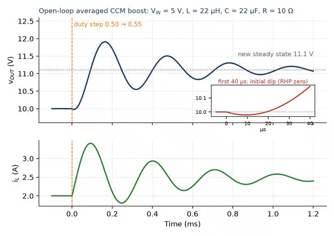
This inverse response is a characteristic of the power stage, not automatically evidence of an incorrectly tuned loop. It constrains achievable control bandwidth, so a CCM boost generally requires a more conservative response-speed target than a buck performing a comparable task. Because ωz falls with increasing D and decreasing R, the control loop must be checked at the minimum input voltage and maximum load, using the actual operating mode rather than one generic bandwidth rule for every boost implementation. [3]
Validate the load steps the system will produce
Steady-state regulation is only part of the requirement. A rail may reach its target voltage yet move outside the permitted range during a real load transition.
Load-step testing should therefore represent the intended system, including the required source conditions and load changes, rather than an arbitrary bench condition. The boost converter design and calculation guide provides complementary component-design detail.
Buck-boost converters: handle input-voltage crossover
Buck-boost conversion addresses a source that can be above or below the required output. This commonly arises in battery-powered systems where discharge and load-induced sag move the source through the target rail voltage, as in the 3.3 V case of Figure 4. [2]
The basic single-switch buck-boost charges the inductor from the input during one interval and delivers stored energy to the output during another. Its basic form produces an inverted output polarity, shown in Figure 8(a).
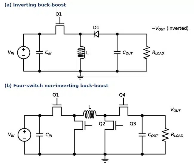
A four-switch non-inverting implementation, Figure 8(b), provides step-down and step-up operation without reversing the output. This adds switching devices and control complexity compared with a basic buck or boost, but no fixed efficiency penalty should be assigned without comparing the actual designs and operating conditions. The crossover region is an important validation point. [2, 5]
Before choosing a buck-boost implementation:
- Define the lowest source voltage at which full regulation is required.
- Include load-induced source sag.
- Establish whether the load requires a non-inverting rail.
- Validate operation while input moves through the output-voltage region, not only at the range endpoints.
Isolated buck: simple auxiliary power with indirect regulation
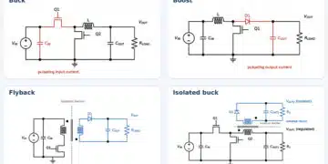
An isolated buck starts with a synchronous buck stage and replaces the ordinary inductor with a coupled magnetic component. A secondary winding, rectifier diode and capacitor provide an isolated output; this implementation is also known as a Fly-Buck converter. Figure 9 shows the arrangement. [4]
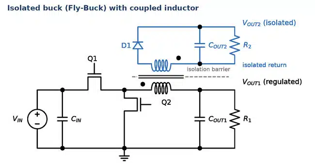
The primary side continues operating as a buck. The isolated rail follows indirectly through magnetic coupling and turns ratio, rather than being directly regulated by a secondary feedback loop.
Applications include auxiliary power for isolated gate drivers, analogue-to-digital converter circuitry, CAN interfaces and RS485 interfaces. The introductory podcast positions this architecture in the approximate 1–15 W range and notes that some applications use only the isolated output. An unused primary output means no external primary-side load; it does not mean that the primary output capacitor or regulation circuit can be omitted. [1, 2, 4]
Turns ratio does not guarantee output accuracy
The control loop directly regulates the primary buck output, not the isolated secondary rail. Secondary voltage depends on the magnetic and rectifier characteristics as well as the relative loading of the outputs. [2, 4]
- Magnetic coupling.
- Winding resistance.
- Leakage inductance.
- Rectifier forward voltage.
- Relative loading of the primary and secondary outputs.
A turns ratio that nominally produces 5 V does not establish a tightly regulated 5 V output under every operating condition. Cross-loading is particularly important: evaluate the outputs as their loads change independently and relative to each other. [2]
A voltage-sensitive secondary load may require a wider permitted supply tolerance or a post-regulator. If post-regulation is used, its input requirements must be included when checking the isolated rail over the specified operating range.
Magnetic substitutions require more than matching inductance
A coupled magnetic component should not be substituted solely on nominal inductance and package size. The winding arrangement, turns ratio, coupling-related behaviour and required insulation function belong in the specification. Output regulation must then be validated in the intended circuit. [2, 4]
The storage-inductor selection guide for DC/DC converters provides broader component-selection context. Coupled magnetics require additional scrutiny because their secondary behaviour and isolation function are not captured by a single inductance value.
Design-in notes for engineers
Translate the architecture decision into a documented electrical, thermal and insulation specification. The following checklist combines the topology-selection framework with the component and implementation considerations developed above. [1–5]
Operating-envelope checklist
- Define isolation by function: personnel protection, ground separation or another system requirement.
- Use power ranges to shortlist architectures, not to establish absolute topology limits.
- Specify the full voltage range presented to the switching stage.
- Select buck, boost or buck-boost from that complete range and confirm the required output polarity.
- Include standby and light-load transitions in buck validation, using the intended controller mode.
- Evaluate boost transient performance with representative load steps and the correct conduction-mode model, including the right-half-plane-zero location at minimum input voltage and maximum load.
- Test buck-boost operation through the input/output crossover.
- Vary isolated-buck primary and secondary loads independently and confirm whether secondary post-regulation is necessary.
- Document required insulation properties separately from nominal output voltage.
- Begin detailed passive-component selection after the architecture satisfies the operating envelope, then iterate if component or thermal constraints invalidate the initial choice.
Datasheet parameters and magnetic-component review
For magnetics, compare inductance and tolerance, winding resistance, current capability, turns ratio where applicable, leakage inductance and the required insulation properties. Confirm how each supplier defines its current ratings and verify the component in the actual converter rather than treating a catalogue rating as a complete circuit qualification. [3, 4]
For capacitors, compare voltage rating, capacitance, equivalent series resistance and ripple-current requirements against the relevant input or output waveform. For switches and rectifiers, check voltage and current stresses alongside loss and thermal requirements. The topology determines the waveforms these components must withstand. [3, 4]
Catalogue versus custom magnetics
For procurement review, use the same electrical, mechanical and insulation specification for catalogue and custom candidates. A catalogue part is suitable only if its documented characteristics satisfy the circuit requirements; a custom part should be supported by an agreed specification and qualification plan.
Record winding connections, turns ratio, inductance conditions, leakage-related requirements and insulation requirements before approving alternatives. Revalidate regulation, temperature and relevant fault behaviour when a substitution changes the magnetic implementation. This is especially important for isolated-buck secondary accuracy and cross-loading. [2, 4]
Qualification and safety
Separate component approval from converter approval. Qualification should cover the intended source and load ranges, start-up, standby transitions, representative transients, temperature and the applicable insulation function. A successful nominal-load demonstration does not establish suitability across those conditions. [2–4]
Where personnel protection is required, establish the applicable end-equipment requirements before approving transformer construction or PCB spacing. Do not accept a generic “isolated” description as a substitute for documented insulation properties. [2]
Limits of the comparison
This article provides an architecture-selection framework rather than a complete converter design. Its application-voltage examples and approximate power ranges illustrate selection logic; the boost worked example illustrates power-stage dynamics with ideal components and is not a component-sizing calculation.
The comparison does not establish inductance values, capacitor ratings, switching frequencies, saturation-current margins, thermal limits or measured efficiency rankings. Detailed design requires the selected controller documentation, magnetic-component data and a power-stage model appropriate to the operating mode. The boost and isolated-buck application reports provide examples of that next level of analysis. [3, 4]
Likewise, the approximate isolated-topology power ranges do not prove that a topology cannot operate beyond the stated range or that another topology is automatically superior within it. Assess the design at its actual source, load, control, thermal and insulation conditions.
Conclusion
SMPS topology selection becomes more reliable when architecture follows requirements rather than familiarity. Isolation, power level and source conditions establish the first shortlist; the complete input-to-output relationship then distinguishes buck, boost and buck-boost.
Isolated auxiliary-power needs may favour an isolated buck, provided its secondary regulation and insulation properties are suitable. For higher-power isolated conversion, forward and LLC deserve comparison with flyback rather than being excluded by habit.
The decisive checks occur beyond nominal conditions. Battery discharge, standby, load transients, voltage crossover and secondary cross-loading determine whether the chosen architecture remains suitable in the real system. Component selection and qualification must preserve that suitability.
FAQ
These answers summarise the selection decisions most relevant to circuit design and component review.
Compare the complete input-voltage range with the required output voltage. Choose buck when the input remains sufficiently above the output, boost when it remains below, and buck-boost when it can cross the output. Then check output polarity, controller limits, light-load behaviour and transient performance. Nominal battery or bus voltage alone is not a sufficient selection criterion.
No. Galvanic isolation establishes separation without a direct conductive connection, but personnel protection requires suitable insulation construction and PCB creepage and clearance for the end equipment. A barrier intended to separate measurement grounds is not automatically suitable for protecting users from hazardous voltages. Document the required insulation function separately from nominal output voltage.
In a conventional boost operating in continuous conduction mode, increasing duty cycle initially shortens the interval during which current reaches the output. Inductor current takes time to increase, so the initial output response opposes the eventual voltage increase. This right-half-plane zero constrains control bandwidth. The corresponding low-frequency discontinuous-conduction model does not have the same behaviour.
Compare alternatives when the required power, semiconductor stress, losses or thermal conditions make the existing flyback approach unattractive. Introductory power ranges can help build a shortlist, but they are not absolute topology limits. Forward changes the energy-transfer arrangement, while LLC uses resonant operation. Neither topology guarantees superior efficiency without checking the actual input, output and load conditions.
Not on inductance alone. Compare winding arrangement, turns ratio, winding resistance, coupling-related behaviour, leakage inductance and required insulation properties. The isolated output is indirectly regulated, so changes can affect secondary voltage and cross-loading performance. Validate the replacement in the intended circuit over the required source, load and temperature conditions before approving the substitution.
How to select an SMPS topology
Use this procedure to produce a defensible shortlist before detailed converter and component design.
Select a converter architecture from its isolation function, complete operating envelope and validation requirements.
- Define the isolation function
Establish whether the converter needs galvanic isolation for personnel protection, ground separation or another system requirement. Record the required insulation function before choosing the magnetic component or PCB spacing.
- Specify the operating envelope
Record minimum and maximum input voltage, required output voltage and polarity, output power and loading of each rail. Include battery discharge, load-induced sag and the voltage actually presented to the switching stage.
- Build the topology shortlist
For non-isolated conversion, select buck, boost or buck-boost from the complete voltage relationship. For isolated conversion, compare isolated buck, flyback, forward and LLC against power, regulation, complexity and stress requirements. Treat published power ranges as guidance rather than limits.
- Review components and control behaviour
Check controller operating modes and limits, magnetic characteristics, capacitor ripple duties and semiconductor stresses. For isolated buck, review turns ratio, leakage-related behaviour, secondary tolerance and any post-regulator requirements before approving catalogue or custom magnetics.
- Validate the complete design
Test the intended source and load range, light-load transitions, representative load steps, input/output crossover and temperature. Vary isolated-buck output loads independently and confirm the required insulation properties before approving the design or a magnetic-component substitution.
Further Reading
These articles develop the magnetic-component and isolated-converter design topics introduced in this selection guide.
- Flyback Converter Design and Calculation — Continue from topology selection to flyback circuit operation and component calculations.
- Flyback Transformer Design: Principles and Calculations — Examine the energy-storage and winding considerations of flyback magnetics.
- Power Inductor Selection: Ferrite vs Powder Cores — Compare core-material trade-offs when selecting power inductors.
- Magnetic Core Materials: Permeability, Losses and Selection — Review how core properties influence magnetic-component selection.
References
References 1 and 2 provide the original selection framework and application examples. The application report and implementation references support the operating-mode, equation, component and layout qualifications.
- Würth Elektronik, Branching Out Beyond the Flyback — Part 1: An Introduction to SMPS and the Decision Tree, Watts Up Podcast, 30 October 2026.
- Würth Elektronik, Buck, Boost, or Bust Through the Topology Trap — Part 2: Choices and Tradeoffs in Non-Isolated SMPS Designs, Watts Up Podcast, 13 November 2026.
- Everett Rogers, Understanding Boost Power Stages in Switchmode Power Supplies, Texas Instruments, application report SLVA061, 1999.
- Vijay Choudhary, AN-2292 Designing an Isolated Buck (Fly-Buck) Converter, Texas Instruments, application report SNVA674C, revised 2014.
- Frederik Dostal, SMPS Topologies and Tips and Tricks, Analog Devices presentation hosted by Würth Elektronik, 2024.
- Würth Elektronik, Analog Devices MAX15062 — Reference Design Search, controller operating-mode description, publication date not stated.
Latest technical review and revision: 16 November 2026.