



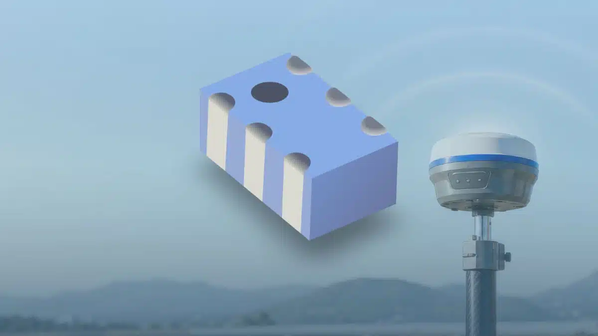
Bourns has introduced the FDP2009N122157H4, a low temperature co‑fired ceramic (LTCC) diplexer targeting compact GNSS L‑band RF front ends where dual‑band isolation, low insertion loss, and PCB area efficiency are critical.
The device integrates distributed inductive and capacitive elements in a monolithic ceramic body, offering designers a predictable, repeatable filter behavior compared with discrete LC implementations in dense layouts.
Introduction
In modern GNSS receivers, multiple L‑band signals (L1, L2, L5) must be separated and recombined with minimal degradation of signal‑to‑noise ratio and without adding unnecessary power consumption or PCB complexity. The FDP2009N122157H4 LTCC diplexer provides a dual‑band filtering function in a single compact component that addresses layout sensitivity and parasitics typically associated with discrete filters, simplifying RF front‑end design for positioning, timing, and satellite‑enabled systems.
Key features and benefits
- LTCC monolithic construction – The diplexer integrates inductive and capacitive elements within a multilayer ceramic structure, which reduces interconnect parasitics and improves consistency of RF characteristics across units and over temperature.
- Dual‑band L‑band operation – Supports two frequency ranges, 1164–1285 MHz (low band) and 1539–1606 MHz (high band), covering GNSS L1, L2, and L5 services without requiring multiple discrete filter networks.
- Low insertion loss – Maximum insertion loss of 1.0 dB at 25 °C (typical 0.56 dB in the low band and 0.87 dB in the high band) helps preserve GNSS receiver sensitivity and improves overall link margin in low‑power RF front ends.
- Stable performance over temperature – Insertion loss remains limited to 1.2 dB maximum over −40 °C to +105 °C, supporting industrial and automotive environments where ambient temperature and self‑heating can vary significantly.
- Compact footprint – A 2.0 × 1.25 × 0.9 mm package minimizes PCB area and enables placement close to the RF input stage, reducing routing length and further limiting unwanted parasitic coupling.
- High isolation and attenuation – Minimum 20 dB attenuation and 20 dB isolation between bands help reduce cross‑band interference and improve selectivity, beneficial in multi‑constellation GNSS receivers and shared‑antenna designs.
- Controlled impedance – A nominal 50 Ω impedance simplifies matching to standard RF front‑end architectures, allowing straightforward integration with LNAs, mixers, and antenna feeds.
- Wide operating temperature range – Rated for −40 °C to +105 °C, the diplexer is suited to industrial and many automotive designs, with stable RF performance in typical outdoor and equipment environments.
- RoHS compliant – Designed to meet current RoHS directives, supporting environmentally compliant designs without special exceptions.
Typical applications
The FDP2009N122157H4 is intended for GNSS RF front‑end integration, and fits in a range of systems where space, repeatability, and low loss matter:
- GNSS receiver RF front ends supporting L1, L2, and L5 bands in multi‑constellation navigation modules.
- GPS‑based positioning and navigation systems in industrial equipment, automotive telematics, and consumer devices.
- Timing synchronization infrastructure in communication networks or industrial control systems where frequency‑selective paths are needed.
- Satellite‑enabled agriculture and surveying equipment that combines high‑precision GNSS with constrained PCB real estate and tough environmental conditions.
- Compact IoT devices and asset‑tracking modules requiring integrated GNSS functionality with shared antenna structures.
Technical highlights
From a design‑in perspective, the key electrical parameters of the FDP2009N122157H4 are summarized below. Exact values should be checked against the manufacturer datasheet.
Electrical performance overview
| Parameter | Value / Range |
|---|---|
| Frequency ranges | 1164–1285 MHz (low band), 1539–1606 MHz (high band) |
| Insertion loss at 25 °C | 1.0 dB max; 0.56 dB typ (low band), 0.87 dB typ (high band) |
| Insertion loss over full temp | 1.2 dB max (−40 °C to +105 °C) |
| Attenuation | 20 dB min |
| Isolation | 20 dB min |
| Return loss | 10 dB min |
| Nominal impedance | 50 Ω |
| Power capacity | 3 W max |
| Operating temperature range | −40 °C to +105 °C |
A low insertion loss in both bands means the diplexer introduces only modest degradation to the system noise figure, which is critical when working with weak satellite signals. The specified minimum isolation and attenuation support clean separation of frequency bands, reducing the risk that strong signals in one band will couple into the other path and desensitize the receiver.
Package and construction
| Attribute | Value |
|---|---|
| Package type | LTCC monolithic diplexer |
| Dimensions (L × W × H) | 2.0 × 1.25 × 0.9 mm |
| Construction | Multilayer ceramic with integrated inductors and capacitors |
The LTCC structure offers a stable dielectric and tightly controlled geometry, which helps maintain the designed filter response over production batches. Compared to building equivalent LC networks from discrete chip inductors and capacitors, the LTCC diplexer reduces PCB routing complexity and sensitivity to layout variations.
Design‑in notes for engineers
To help RF and hardware engineers integrate the FDP2009N122157H4 efficiently, several practical points are worth considering:
- Placement close to the RF input or LNA – Position the diplexer as close as possible to the antenna feed or LNA input to minimize trace length and reduce parasitic inductance and capacitance, which can distort the intended filter response.
- Impedance matching and terminations – Although the device is specified for nominal 50 Ω systems, verify the matching network around the diplexer using S‑parameter simulations. Pay attention to the return loss specification and confirm that your PCB layout maintains the target impedance across the operating bands.
- PCB layout and ground referencing – Use solid ground referencing under and around the component, following any manufacturer layout guidelines in the datasheet. Poor ground via placement or discontinuities can introduce unwanted coupling and degrade isolation between the low‑band and high‑band ports.
- Thermal and power considerations – While rated up to 3 W, most GNSS applications operate at relatively low RF power levels. Nonetheless, check that worst‑case conditions in your design (for example, test modes or fault scenarios) remain below the specified power capacity and within the operating temperature range.
- Manufacturing and tolerance awareness – Because the diplexer integrates the full filter structure, RF performance is less dependent on external component tolerances. However, it is still good practice to review process variation data provided in the datasheet and, if needed, characterize several units to understand margin in your particular layout.
- EMC and co‑existence – In systems where GNSS shares an antenna or PCB space with other RF services, the diplexer’s isolation and attenuation characteristics can help manage coexistence. Evaluate the filter behavior not only at the nominal bands but also at nearby interference frequencies, using the detailed frequency response curves from the datasheet.
- Qualification for environment – The specified temperature range and RoHS compliance support industrial and many automotive uses. For safety‑critical or “lifesaving” applications, note the manufacturer’s general disclaimers and confirm the suitability of the device against system‑level standards and reliability expectations.
Source
The information in this article is based on the manufacturer’s official press release and associated technical documentation for the FDP2009N122157H4 LTCC diplexer, with added editorial context for practical design‑in and application use. Exact numerical values and limits should always be verified against the latest manufacturer datasheet before final design commitments.