


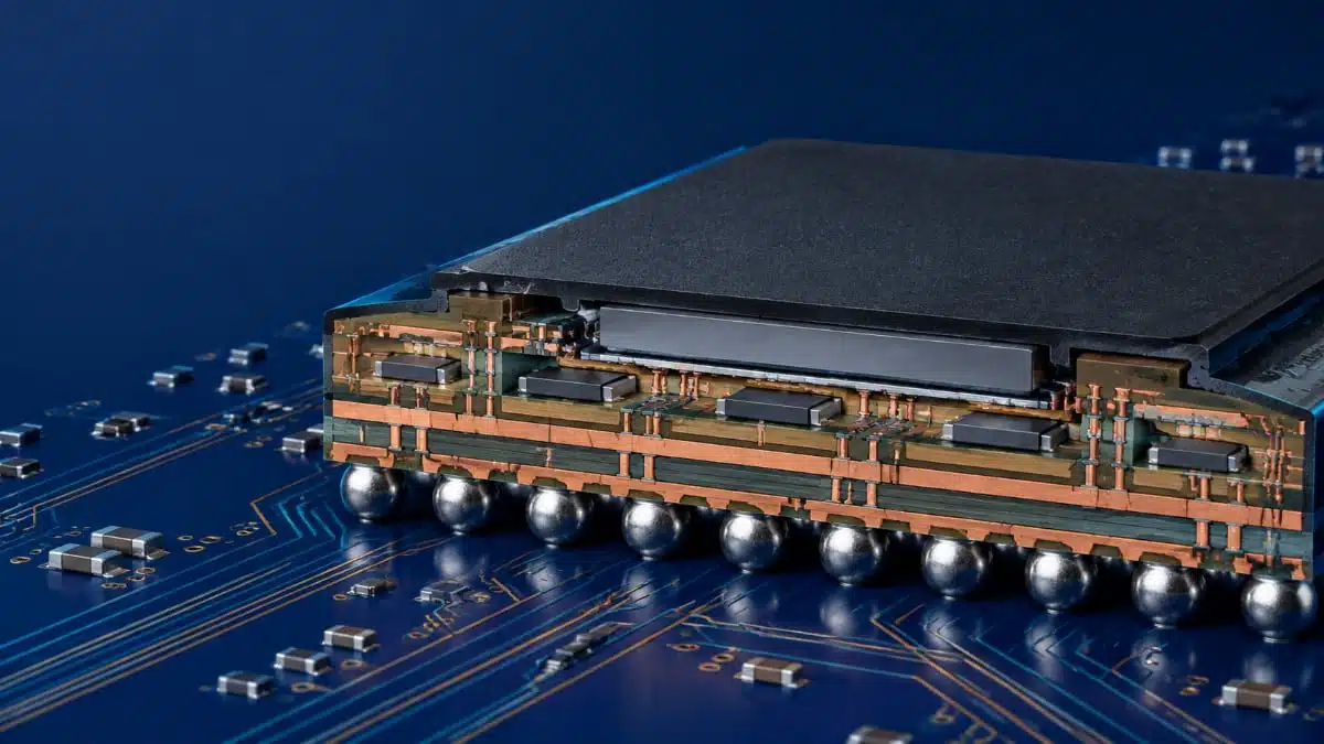
LG Innotek has demonstrated flip-chip ball grid array (FC-BGA) substrate samples that embed silicon capacitors within the package substrate for AI semiconductor applications.
The announced approach places the capacitor closer to the chip power connection, targeting reduced interconnect parasitics and additional surface-area flexibility at package level.
Key features and benefits
- Embedded silicon capacitors in FC-BGA substrates: LG Innotek showed structures with silicon capacitors located in either the substrate core or a buildup layer.
- Two integration approaches: The core-layer implementation accommodates relatively thicker, higher-capacitance silicon capacitors, while the buildup-layer approach uses thinner devices to limit overall substrate thickness.
- Configurable placement: The manufacturer states that capacitor location and specifications can be selected according to the semiconductor and substrate design.
- Near-die power decoupling: Moving a decoupling element from the substrate surface into the package shortens the electrical path to the semiconductor. In a fast transient load event, this can help reduce parasitic inductance in the power-delivery network.
- Surface-area release: Embedded components can free package-substrate surface area for other routing, components, or mechanical constraints.
Silicon capacitors are fabricated with semiconductor processing on a silicon substrate, commonly using integrated metal-insulator-metal or related structures. Their suitability for package-level decoupling is linked to compact geometry and low parasitic inductance; see the Silicon and Silicon Wafer Based Integrated Capacitors technology overview.
Technical highlights
| Aspect | Manufacturer-reported information | Engineering relevance |
|---|---|---|
| Package technology | FC-BGA substrate with embedded silicon capacitors | Targets package-level power distribution for high-performance semiconductor devices |
| Capacitor locations | Substrate core layer or buildup layer | Placement affects thickness, routing, power/ground connection length, thermal path, and manufacturability |
| Core-layer option | Supports relatively thick, high-capacitance silicon capacitors | May be useful where capacitance density is prioritised, subject to substrate stack-up constraints |
| Buildup-layer option | Uses thinner silicon capacitors to reduce total substrate thickness | Can support thinner package structures, but final electrical and mechanical constraints must be verified |
| Intended context | AI semiconductors requiring stable power delivery | Relevant to high-current, fast-load-transient processor and accelerator rails |
| Additional development | Embedding of active devices and bridges is under development | No electrical specifications, qualification status, or product-release details are provided for these structures |
The announcement does not publish part numbers, capacitance values, voltage ratings, ESR, ESL, dielectric system, dimensions, thermal limits, reliability-test conditions, substrate materials, or qualification data. These parameters must be confirmed in current manufacturer documentation before a component or package architecture is selected.
Application fit
The technology is relevant to advanced package-level power delivery rather than conventional board-level capacitor placement. It may be considered where the load current changes rapidly and the inductance between the capacitor and semiconductor supply terminals becomes a critical part of the PDN impedance.
| System area | Potential role of embedded silicon capacitance | What must still be assessed |
|---|---|---|
| AI accelerators and high-performance processors | High-frequency local decoupling close to power bumps or package connections | Target impedance, transient-current spectrum, rail voltage, package parasitics, and regulator control-loop interaction |
| Advanced FC-BGA packages | Integration of decoupling within the package substrate | Stack-up, via and plane design, routing density, warpage, assembly yield, and inspectability |
| Server and data-centre boards | Part of a hierarchical PDN alongside board-level capacitors and voltage regulators | Division of capacitance across package, board, and bulk-energy-storage levels |
| Multi-chip package architectures | Potential local support for power delivery around logic or memory dies | Die-specific current profiles, coupling between rails, thermal gradients, and interconnect constraints |
Embedded silicon capacitors do not replace bulk or intermediate-frequency capacitors elsewhere in the system. AI hardware normally requires a hierarchical PDN, with energy storage distributed across the voltage-regulator, board, package, and die levels; Murata Publishes Power Delivery Guide for AI Servers provides related system-level context.
Design-in notes for engineers
- Model the complete PDN: Evaluate package, PCB, socket or connector, voltage-regulator module, and load together. A low-inductance capacitor can be limited by the inductance of planes, vias, bumps, and connections around it.
- Obtain impedance data at the correct reference plane: Capacitance alone is insufficient. Confirm frequency-dependent impedance, ESR, ESL, resonances, measurement fixtures, mounting or embedding conditions, and the relevant DC bias.
- Check the rail transient requirement: Validate against the processor or ASIC power-integrity specification, including load-step amplitude, edge rate, allowed voltage excursion, rail coupling, and power-sequencing conditions.
- Confirm stack-up constraints: Core-layer and buildup-layer integration impose different thickness, routing, lamination, via, thermal, and fabrication constraints. The manufacturer’s announcement does not provide these values.
- Review mechanical reliability: Package warpage, coefficient-of-thermal-expansion mismatch, temperature cycling, moisture exposure, reflow compatibility, drop or bend conditions, and board-level reliability must be addressed under the final assembly conditions.
- Validate thermal performance: Determine capacitor losses, local heat generation, thermal paths, die temperature, and possible impact on nearby interconnects or active devices.
- Confirm manufacturing control: For production release, clarify supplier qualification, substrate-fabrication process capability, test coverage, traceability, failure analysis, and repair or rework limitations.
- Do not assume equivalence with MLCCs: Embedded silicon capacitors and low-inductance ceramic capacitors for high-speed decoupling can address related PDN requirements, but their integration method, parasitics, available capacitance, voltage capability, and reliability evidence require separate validation.
- Use current documentation for release: The public announcement does not specify final product configurations or qualification conditions. Current LG Innotek datasheets, substrate specifications, drawings, and customer-specific package documentation should control final selection and release.
Further reading
- Silicon and Silicon Wafer Based Integrated Capacitors
- Murata Publishes Power Delivery Guide for AI Servers
- Understanding AI Passive Components and Interconnects
- Analysis of Multi-Layer Ceramic Capacitors used in Power Distribution Networks
Source
This article is based on the published report covering LG Innotek’s FC-BGA substrate demonstration with embedded silicon capacitors. The available announcement does not include a current LG Innotek datasheet or detailed qualification documentation; engineers should obtain current manufacturer specifications before component selection, package design, qualification, and production release.