




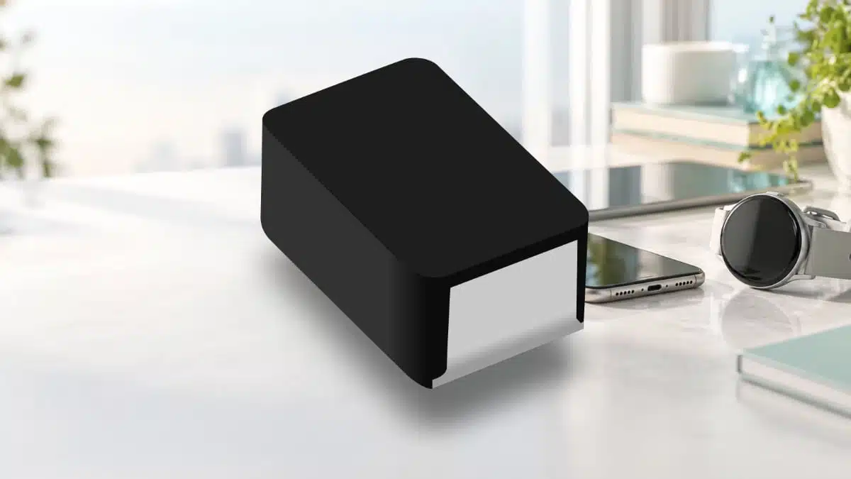
Bourns has introduced the SRP201210V Series, a family of shielded SMD power inductors for compact portable power converters.
The new series combines a 2.0 mm × 1.2 mm footprint with a 1.0 mm maximum profile, addressing converter layouts where inductor height, board area and current capability must be balanced. Power inductors remain a critical constraint in compact DC-DC converter layouts because both magnetic saturation and self-heating can limit usable current.
Key features and benefits
- Magnetically shielded construction for reduced external magnetic-field radiation in dense PCB assemblies
- 2.0 mm × 1.2 mm footprint with 1.0 mm maximum height
- Inductance options from 0.24 µH to 0.47 µH
- ±20% inductance tolerance
- −55 °C to +125 °C operating-temperature range
- Typical DC resistance from 13 mΩ to 21 mΩ, depending on inductance value
- Maximum DC resistance from 17 mΩ to 24 mΩ
- RoHS-compliant and halogen-free construction
The announcement positions the family for wearable devices, mobile electronics, compact IoT modules, portable battery-powered equipment and solid-state drives. These are plausible placement areas for a low-profile power inductor, but final suitability depends on the converter’s switching frequency, DC-bias requirement, ripple current, thermal environment and magnetic-field sensitivity.
Technical highlights
| Parameter | SRP201210V Series | Selection relevance |
|---|---|---|
| Inductance range | 0.24 µH – 0.47 µH | High-current converter stages |
| Inductance tolerance | ±20% | Control-loop and ripple design |
| Footprint | 2.0 mm × 1.2 mm | Dense PCB layouts |
| Maximum height | 1.0 mm | Thin portable assemblies |
| Operating temperature | −55 °C to +125 °C | Ambient and self-heating margin |
| Typical DCR | 13 mΩ – 21 mΩ | Conduction-loss estimate |
| Maximum DCR | 17 mΩ – 24 mΩ | Worst-case loss analysis |
| Typical | 4.7 A – 5.9 A | Thermal current capability |
| Maximum | 4.2 A – 5.2 A | Worst-case current check |
| Typical | 5.5 A – 7.6 A | Peak-current margin |
| Maximum | 5.0 A – 7.0 A | Worst-case saturation margin |
| Typical SRF | ≥120 MHz | High-frequency parasitic behaviour |
| Maximum ACR at 1 MHz, 1 V | 80 mΩ – 170 mΩ | Switching-loss assessment |
The published data distinguishes RMS and saturation-current values. RMS current is relevant to winding loss and temperature rise, while saturation current relates to DC-bias-induced inductance reduction. Inductor saturation current should therefore be checked against the converter’s maximum peak current, not merely its nominal load current.
The released electrical table lists series-level ranges but does not identify individual orderable part numbers or the exact test definitions for , , inductance measurement frequency, temperature rise or inductance-drop criterion. These points should be confirmed in the current part-level datasheet before production release.
Typical applications
The published ratings support use in compact, high-current switched-mode power stages where the required inductance falls within the 0.24 µH to 0.47 µH range.
| Application position | Relevant published ratings | Design consideration |
|---|---|---|
| Point-of-load buck converter | 0.24 µH – 0.47 µH, up to 7.0 A maximum | Check peak inductor current |
| Battery-powered converter | 1.0 mm maximum height, low DCR | Assess efficiency at battery voltage |
| Wearable power rail | 2.0 mm × 1.2 mm footprint, shielded construction | Check nearby sensor coupling |
| Mobile-device regulator | 4.2 A – 5.2 A maximum | Verify copper and thermal spreading |
| Compact SSD power stage | Shielded construction, ≥120 MHz typical SRF | Validate conducted and radiated EMC |
The low inductance range is most relevant to high-current, low-voltage buck converters and similar point-of-load stages. A 0.24 µH or 0.47 µH value cannot be selected from load current alone: switching frequency, input-output voltage ratio, allowable ripple current, control-loop design and transient requirements determine the required inductance.
Application fit
The 1.0 mm maximum profile makes the SRP201210V Series relevant where enclosure clearance limits magnetic-component height. The 2.0 mm × 1.2 mm footprint also helps preserve PCB area in tightly packed modules, though the surrounding copper area required to manage inductor and converter heat must still be retained.
The metal-alloy powder core and magnetic shielding are relevant where neighbouring circuits are sensitive to magnetic coupling. Shielding reduces stray field, but it does not eliminate switching-node electric-field coupling, conducted noise, layout-related loop area or converter ringing. EMC performance must be assessed at the complete board level.
No AEC-Q200 qualification, safety approval, humidity qualification, lifecycle notice, SPICE model, S-parameter data, impedance curves, DCR-versus-temperature curve, outline drawing or recommended land-pattern document was identified in the official material reviewed for this release. Those omissions should not be interpreted as evidence that such documents do not exist; they were not publicly located during this source sweep.
Design-in notes for engineers
- Select inductance from the converter’s required ripple-current range, switching frequency and operating voltage range rather than from package size alone.
- Use the maximum value of 5.0 A to 7.0 A for worst-case peak-current screening, after confirming the datasheet’s inductance-drop criterion and measurement temperature.
- Use the maximum value of 4.2 A to 5.2 A for thermal screening, then verify temperature rise on the finished PCB under worst-case ambient conditions.
- Calculate winding loss using maximum DCR, including DCR rise with temperature where the current datasheet provides that information.
- Evaluate AC loss at the actual switching frequency. The published ACR specification is measured at 1 MHz and 1 V, so it cannot be directly substituted for loss at a different ripple-current waveform or frequency.
- Keep the converter’s hot loop compact and place input ceramic capacitors close to the switching devices. Shielding in the inductor does not compensate for a large, noisy power-loop area.
- Confirm solder land pattern, reflow limits, board flex exposure and enclosure clearance before layout freeze.
- Validate saturation margin, thermal rise, output ripple and conducted/radiated emissions under startup, load transient, overload and fault conditions. This does not replace system-level validation.
Further reading
- Power Inductors and Storage Chokes
- Saturation Current of Inductors and its Measurement
- Storage Inductors Selection for DC/DC Converters
- Inductors Modeling with LTSpice
Source
This information is based on the Bourns SRP201210V Series press release and official Bourns product documentation located during the source review. Engineers should consult the current manufacturer datasheet and any applicable package, mounting and qualification documentation before final component qualification and design release.