


The Silicon Motherboard (Si-MB) from Nisshinbo Micro Devices is a 3D mounting technology that places ICs, passive elements formed in the silicon and external chip passives in one package.
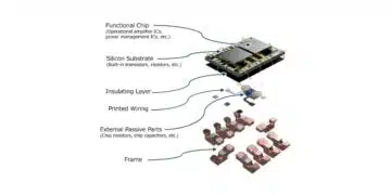
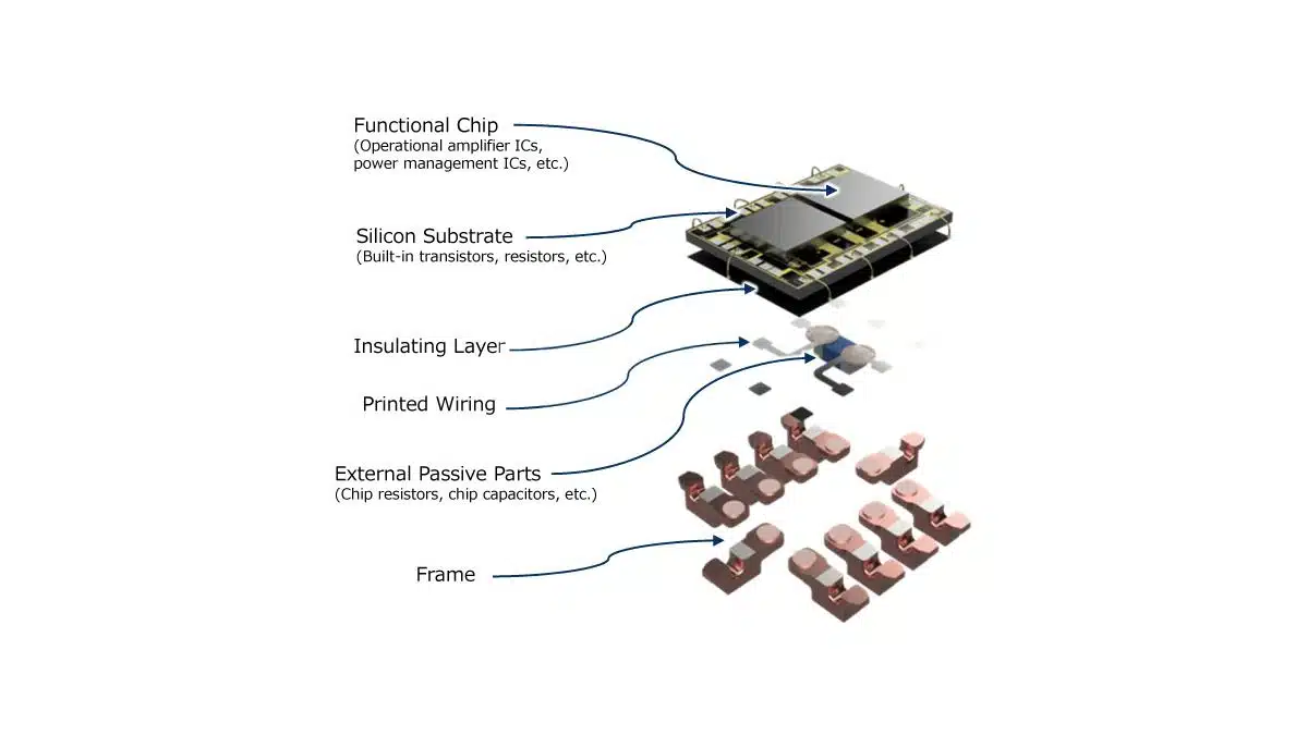
Nisshinbo Micro Devices has developed the Si-MB to consolidate analog ICs and their peripheral components in an existing mass-production package outline. Functional chips sit on the top surface of a silicon substrate, resistors, capacitors and transistors are formed inside the substrate by wafer processing, and external passive components are mounted on the bottom side. In a window-comparator prototype the mounting footprint is about 80 % smaller than the equivalent discrete configuration.
Key Features and Benefits
- Both sides of the silicon substrate are used: functional chips on top, external passive components on the bottom.
- Built-in elements: transistors, resistors and capacitors formed inside the substrate by wafer processing.
- External passives: capacitors above 1,000 pF, resistors below 1 Ω and inductors can be mounted on the bottom side.
- Existing package shapes: mass-production package outlines are reused, so existing mounting equipment applies.
- Application range: consumer, industrial and automotive electronics.
- Prototype result: window comparator with about 80 % smaller mounting footprint than the discrete configuration.
Technical Highlights
| Parameter | Silicon Motherboard (Si-MB) |
|---|---|
| Technology | 3D mounting, circuits on both sides of a silicon substrate |
| Top side | Functional chips, e.g. operational amplifier and power management ICs |
| Inside the substrate | Transistors, resistors, capacitors (wafer process) |
| Bottom side | External chip resistors, chip capacitors and inductors |
| External capacitors | Above 1,000 pF |
| External resistors | Below 1 Ω |
| Package | Existing mass-production package outline |
| Prototype | Window comparator, two comparator ICs, two external chip resistors |
| Footprint reduction | About 80 % versus discrete configuration (prototype) |
Structure
The package stacks a functional chip layer, the silicon substrate, an insulating layer, printed wiring, external passive parts and a frame. The silicon substrate carries the built-in transistors and resistors, while the printed wiring on its underside connects the external chip resistors and chip capacitors.
Chiplet technology concentrates on stacking IC chips and does not readily accommodate chip resistors or capacitors. Higher packing density in chiplets also comes with limited durability, which restricts the application range. The Si-MB addresses both points by adding a passive-component layer and by using proven package outlines.
Window-Comparator Prototype
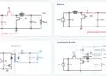
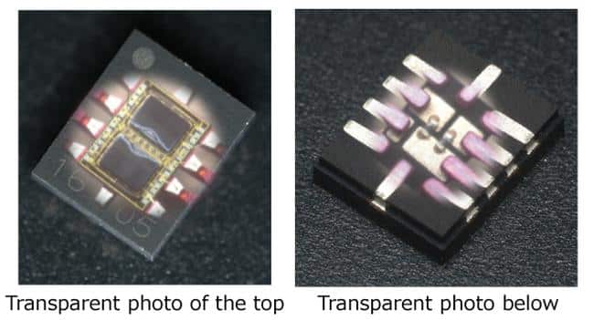
The prototype combines two comparator ICs on the silicon substrate, resistive elements formed inside the substrate and two chip resistors on the printed wiring underside. A window comparator uses two comparators and a resistor network to detect whether a signal lies inside or outside a voltage window. Reference and divider resistors determine the thresholds. The footprint of the integrated version is about 80 % smaller than the same function built from discrete parts.
Typical Applications
Target applications are consumer, industrial and automotive electronics where several ICs and peripheral components are consolidated into one part.
- Analog signal chains: operational amplifiers and comparators whose accuracy depends on the surrounding resistors, such as gain-setting, divider and threshold networks.
- Power management: power management ICs with bottom-side capacitors above 1,000 pF and current-sense resistors below 1 Ω.
- Industrial equipment: a single component replaces several parts in procurement and stock keeping.
- Automotive and high-reliability applications: the existing mass-production package outlines are the basis for use where durability is required.
Application Fit
Silicon-integrated passives are covered in the Silicon Capacitors and Integrated Passives Dossier. Capacitors above 1,000 pF, low-resistance resistors and inductors are difficult to install in conventional chiplets. The Si-MB adds a second route: capacitors above 1,000 pF, resistors below 1 Ω and inductors are mounted as external chip parts on the bottom side of the same substrate.
Embedded silicon capacitors for AI processors follow the same direction of moving passives into the semiconductor package. The Si-MB applies it to analog ICs and their peripheral networks.
Consolidation shifts parts from the bill of materials of the board to that of the module. Resistor and capacitor values, tolerances and temperature coefficients are then fixed by the module specification. They cannot be changed on the board.
Design-In Notes for Engineers
- Module datasheet: the electrical characteristics of the integrated passive network, including tolerance, temperature drift and matching, are those of the module and should be compared with the discrete design.
- Footprint comparison: the 80 % footprint reduction applies to the window-comparator prototype. The saving for other functions depends on the number and size of the replaced discrete parts.
- Thermal and power: resistors below 1 Ω in a current-sense role dissipate power in the package, so the thermal budget of the module needs to be assessed together with the IC.
- Assembly: the package outline is an existing mass-production shape, so placement, reflow and inspection follow the standard process of that package.
- Second source: discrete parts can be replaced from several suppliers, while an integrated module is tied to one source. Supply and lifecycle planning should reflect this.
- Final selection should be validated under the actual operating conditions.
Further Reading
- Imec Presents High-density MIMCAP RF interposer for III-V chiplets
- Samsung Presents Ultra‑Thin Silicon Capacitors for AI and Server PDN
- Empower Releases High-Density Embedded Silicon Capacitors
Source
This article is based on the Nisshinbo Micro Devices product announcement and official product documentation. Engineers should refer to the current manufacturer datasheet for final design and qualification.
References
- The world’s first technology ‘Silicon Motherboard’: Circuits are formed on both sides of the silicon substrate, reducing mounting footprint by 80%, Nisshinbo Micro Devices Inc., 19 August 2026.