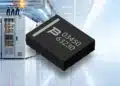










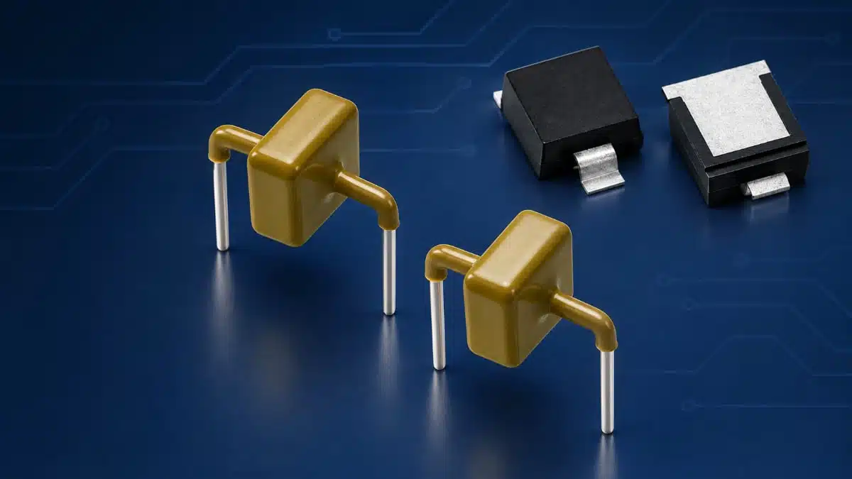
Littelfuse has introduced the AK-FB and AK-A high-power transient voltage suppressor diode families for overvoltage protection in high-voltage DC systems.
The Littelfuse AK-FB devices use controlled-foldback behaviour, while the AK-A devices use non-foldback avalanche clamping. Both families target protection of SiC, GaN and silicon power switches against surge and switching transients.
Key features and benefits
- AK-FB peak pulse current options of 3, 6, 8 and 10 kA.
- AK-A peak pulse current options of 1, 3 and 6 kA.
- Pulse-current ratings tied to an 8/20 µs waveform, rather than continuous conduction.
- Controlled-foldback operation in AK-FB, with minimum snapback voltage at or above reverse standoff voltage.
- Bidirectional axial-leaded devices, with reflow and wave-soldering capability.
- Bulk packaging of 56 devices, with additional 12-device packaging options for AK6-FB, AK8-FB and AK10-FB.
The central selection issue is the relationship between normal bus voltage and the voltage reaching the protected semiconductor during a transient. A high surge-current rating does not replace the need to check the device’s standoff, breakdown and loaded clamping voltages.
Technical highlights
Controlled foldback versus avalanche clamping
The AK-FB family uses a controlled-foldback current–voltage characteristic to maintain near-constant clamping voltage during transient conduction. Its minimum snapback voltage remains at or above the reverse standoff voltage, avoiding DC-supply latch-up within the device’s rated operating conditions.
The AK-A family uses traditional avalanche clamping without foldback. Selection therefore involves different current–voltage behaviour, not simply a choice between surge-current ratings.
For TVS diode protection, three voltage parameters serve different purposes:
- Reverse standoff voltage defines the normal working-voltage boundary.
- Breakdown voltage characterises the onset of conduction at a defined test current.
- Clamping voltage defines the voltage across the TVS at a defined surge current and waveform.
These parameters should remain separate throughout component selection and protection-margin calculations.
Representative electrical ratings
The following devices illustrate the available combinations of working voltage and surge-current capability. Maximum clamping values apply at the indicated peak pulse current with an 8/20 µs waveform and an ambient temperature of 25 °C.
| Part number | Reverse standoff voltage | Peak pulse current | Maximum clamping voltage |
|---|---|---|---|
| AK3-430C-FB | 430 V | 3 kA | 580 V |
| AK6-700C-FB | 700 V | 6 kA | 870 V |
| AK8-450C-FB | 450 V | 8 kA | 568 V |
| AK8-470C-FB | 470 V | 8 kA | 580 V |
| AK10-550C-FB | 550 V | 10 kA | 786 V |
| AK3-430C-A | 430 V | 3 kA | 635 V |
| AK3-860C-A | 860 V | 3 kA | 1272 V |
| AK6-240C-A | 240 V | 6 kA | 451 V |
| AK6-430C-A | 430 V | 6 kA | 740 V |
The AK8-470C-FB, for example, combines a 470 V reverse standoff voltage with a maximum clamp of 580 V at 8 kA. Its breakdown-voltage range is 483–537 V at a test current of 10 mA. The 580 V clamp value—not the standoff or breakdown voltage—sets the device-level transient voltage for that rated surge condition.
The AK6-700C-FB has a 700 V minimum snapback voltage and a breakdown range of 760–825 V at 10 mA. Its maximum reverse leakage is 10 µA at the reverse standoff voltage, while maximum capacitance is 0.7 nF at zero bias and 10 kHz.
Temperature, construction and assembly
AK3-FB, AK6-FB, AK8-FB, AK10-FB, AK3-A and AK6-A have operating junction-temperature ranges of −55 °C to +125 °C and storage-temperature ranges of −55 °C to +150 °C. Their surge capability depends on initial junction temperature and pulse duration, so elevated-temperature selection requires the corresponding derating and pulse-power curves.
These devices use glass-passivated junctions and silver-plated leads. Reflow and wave soldering are supported, but the assembly profiles differ and should be matched to the selected process.
Mechanical dimensions vary by sub-family and voltage option. For example, the AK8-FB outline dimension G is 17.5 ± 1.5 mm for AK8-450C-FB and 18.5 ± 1.5 mm for AK8-470C-FB. Layout work should therefore use the individual device outline rather than a generic AK-family footprint.
Environmental test conditions for these sub-families include 1008 hours at 85 °C and 85% relative humidity, with reverse bias at 80% of rated breakdown voltage, under JESD22-A-101. These are component stress-test conditions, not an operating-lifetime rating.
Typical applications
Target applications include:
- HVDC converters and power supplies.
- Battery energy storage systems.
- AI, data centre and ICT HVDC distribution.
- Solid-state transformers.
- Solid-state circuit breakers.
- EV chargers and rolling-stock power electronics.
For converter and power-supply protection, reverse standoff voltage must exceed the maximum normal voltage across the TVS, while the loaded clamping voltage must remain compatible with the protected circuit’s transient limits. The 700 V standoff and 870 V maximum clamp of AK6-700C-FB illustrate why both values matter: the working-voltage rating is not the residual voltage during a surge.
In solid-state circuit breakers, turn-off transients make the protection interconnection part of the clamping circuit. Stray inductance between an external TVS and the semiconductor can increase the voltage at the switch above the voltage measured directly across the suppressor. TVS placement and connection symmetry therefore affect the protection achieved in the assembled breaker.
Design-in notes for engineers
- Select reverse standoff voltage above the highest normal voltage across the protection node, including operating tolerances and legitimate excursions.
- Compare semiconductor transient limits with the maximum clamping voltage at the required current and waveform, rather than with breakdown voltage.
- Evaluate pulse duration, absorbed surge energy and initial junction temperature together. Apply the selected device’s derating characteristics.
- Keep the surge-current path short and minimise interconnection inductance. Assess voltage directly at the protected semiconductor.
- Use the exact part outline for mounting dimensions and lead geometry, and match the soldering process to its assembly profile.
- Account for the typical short-circuit failure mode following excessive voltage or current when coordinating system fault protection.
- Validate the completed protection circuit under actual operating and transient conditions before production release.
Further reading
- Overvoltage Protection Devices Selection Guidelines
- Overvoltage and Transient Protection for DC/DC Power Modules
- Circuit Protection Selection Guide
Source
This article is based on the Littelfuse product announcement and official product documentation. Engineers should refer to the current manufacturer datasheet for final design and qualification.
References
- Littelfuse Launches AK-FB and AK-A Series High-Power TVS Diodes for High-Voltage DC (HVDC) Applications, Littelfuse, November 12, 2026.
- AK3-FB Series Datasheet, Littelfuse, October 16, 2026.
- AK6-FB Series Datasheet, Littelfuse, July 7, 2026.
- AK8-FB Series Datasheet, Littelfuse, September 11, 2026.
- AK10-FB Series Datasheet, Littelfuse, September 11, 2026.
- AK3-A Series Datasheet, Littelfuse, September 21, 2026.
- AK6-A Series Datasheet, Littelfuse, September 22, 2026.
- An Introduction to Transient Voltage Suppression Devices, Littelfuse, September 19, 2016.
- Overvoltage Protection for Power Semiconductors in Solid-State DC Breakers for BESS and Datacenter Applications, Littelfuse, 2025.