







Passive Components Blog
No Result
View All Result
  • Home
  • News
    • All
    • Aerospace & Defence
    • Antenna
    • Applications
    • Automotive
    • Capacitors
    • Circuit Protection Devices
    • electro-mechanical news
    • Filters
    • Fuses
    • Inductors
    • Industrial
    • Integrated Passives
    • inter-connect news
    • Market & Supply Chain
    • Market Insights
    • Medical
    • Modelling and Simulation
    • New Materials & Supply
    • New Technologies
    • Non-linear Passives
    • Optoelectronics and Isolation
    • Oscillators
    • Passive Sensors News
    • Resistors
    • RF & Microwave
    • Telecommunication
    • Weekly Digest
    VACUUMSCHMELZE VACODUR Max cobalt-iron lamination material illustrated as thin metallic rotor and stator stacks.

    VACUUMSCHMELZE Introduced VACODUR Max Cobalt-Iron Alloy for Motor Laminations

    Stackpole RPCQ thick-film chip resistors in rectangular surface-mount packages with end terminations

    Stackpole Releases Pulse-Withstanding Chip Resistors up to 4 W

    Bourns CRT-G thin film chip resistor illustration with a rectangular body and metallic end terminations

    Bourns Introduces Precision Thin Film Resistors for Measurement

    Würth Elektronik ABC of Thermal Management textbook

    Würth Elektronik Launches ABC of Thermal Management Guide

    Schematic of six-arm nitrene crosslinker joining PEI polymer chains in a free-standing dielectric film.

    Crosslinked PEI Film Capacitor Dielectrics Reach 6 J/cm³ at 200°C

    Conceptual illustration of Peak Nano NanoPlex HDC capacitor dielectric film rolls beside a cast-film production line

    Peak Nano Scales NanoPlex HDC Capacitor Film Production 20-Fold

    Bourns Releases 450 V DC Bus TVS Diode

    YAGEO Nexensos M422 Pb-free platinum RTD graphic showing the operating temperature range, nominal resistance options and joining methods.

    YAGEO Introduces Pb-Free Platinum RTD Temperature Sensor

    Reference tantalum capacitor anode characterization, tantalum anode modeling, process selection and life-test verification.

    Tantalum Anode Design Combines Structural Benchmarks and Modeling

    Trending Tags

    • Ripple Current
    • RF
    • Leakage Current
    • Tantalum vs Ceramic
    • Snubber
    • Low ESR
    • Feedthrough
    • Derating
    • Dielectric Constant
    • New Products
    • Market Reports
  • Knowledge Blog
  • Dossiers
    • Aerospace and Defense Passive Components Dossier
    • AI Hardware Dossier
    • Automotive Dossier
    • Industrial Robotics Dossier
    • Power Converter Dossier
    • Capacitor Dossier
    • Circuit Protection Dossier
    • Inductor Dossier
    • Resistor Dossier
    • Silicon Capacitors and Integrated Passives Dossier
  • Suppliers
    • Who is Who
  • PCNS
    • PCNS 2025
    • PCNS 2023
    • PCNS 2021
    • PCNS 2019
    • PCNS 2017
  • Events
  • Home
  • News
    • All
    • Aerospace & Defence
    • Antenna
    • Applications
    • Automotive
    • Capacitors
    • Circuit Protection Devices
    • electro-mechanical news
    • Filters
    • Fuses
    • Inductors
    • Industrial
    • Integrated Passives
    • inter-connect news
    • Market & Supply Chain
    • Market Insights
    • Medical
    • Modelling and Simulation
    • New Materials & Supply
    • New Technologies
    • Non-linear Passives
    • Optoelectronics and Isolation
    • Oscillators
    • Passive Sensors News
    • Resistors
    • RF & Microwave
    • Telecommunication
    • Weekly Digest
    VACUUMSCHMELZE VACODUR Max cobalt-iron lamination material illustrated as thin metallic rotor and stator stacks.

    VACUUMSCHMELZE Introduced VACODUR Max Cobalt-Iron Alloy for Motor Laminations

    Stackpole RPCQ thick-film chip resistors in rectangular surface-mount packages with end terminations

    Stackpole Releases Pulse-Withstanding Chip Resistors up to 4 W

    Bourns CRT-G thin film chip resistor illustration with a rectangular body and metallic end terminations

    Bourns Introduces Precision Thin Film Resistors for Measurement

    Würth Elektronik ABC of Thermal Management textbook

    Würth Elektronik Launches ABC of Thermal Management Guide

    Schematic of six-arm nitrene crosslinker joining PEI polymer chains in a free-standing dielectric film.

    Crosslinked PEI Film Capacitor Dielectrics Reach 6 J/cm³ at 200°C

    Conceptual illustration of Peak Nano NanoPlex HDC capacitor dielectric film rolls beside a cast-film production line

    Peak Nano Scales NanoPlex HDC Capacitor Film Production 20-Fold

    Bourns Releases 450 V DC Bus TVS Diode

    YAGEO Nexensos M422 Pb-free platinum RTD graphic showing the operating temperature range, nominal resistance options and joining methods.

    YAGEO Introduces Pb-Free Platinum RTD Temperature Sensor

    Reference tantalum capacitor anode characterization, tantalum anode modeling, process selection and life-test verification.

    Tantalum Anode Design Combines Structural Benchmarks and Modeling

    Trending Tags

    • Ripple Current
    • RF
    • Leakage Current
    • Tantalum vs Ceramic
    • Snubber
    • Low ESR
    • Feedthrough
    • Derating
    • Dielectric Constant
    • New Products
    • Market Reports
  • Knowledge Blog
  • Dossiers
    • Aerospace and Defense Passive Components Dossier
    • AI Hardware Dossier
    • Automotive Dossier
    • Industrial Robotics Dossier
    • Power Converter Dossier
    • Capacitor Dossier
    • Circuit Protection Dossier
    • Inductor Dossier
    • Resistor Dossier
    • Silicon Capacitors and Integrated Passives Dossier
  • Suppliers
    • Who is Who
  • PCNS
    • PCNS 2025
    • PCNS 2023
    • PCNS 2021
    • PCNS 2019
    • PCNS 2017
  • Events
No Result
View All Result
Passive Components Blog
No Result
View All Result

Samsung Electro-Mechanics Patent Targets to Reduce Moisture and Cracks in High-Capacity MLCCs

26.10.2026
Reading Time: 5 mins read
A A
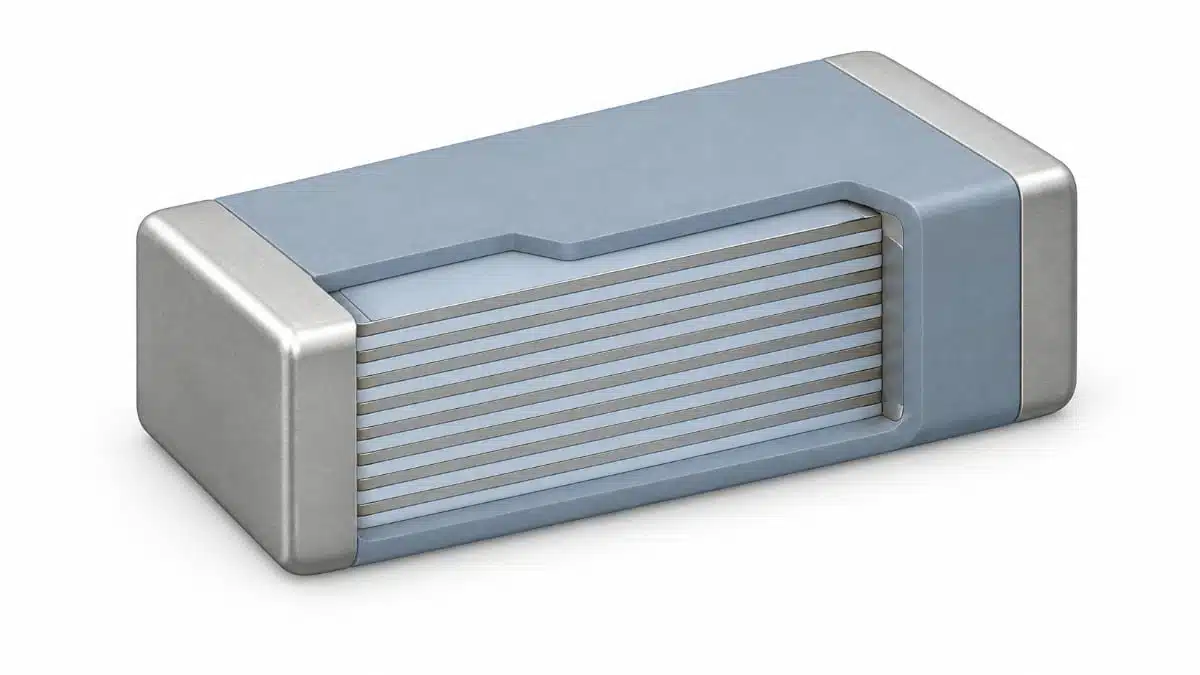
MLCC construction image

Samsung Electro-Mechanics has disclosed an MLCC construction that combines a four-surface dielectric protection layer with internal electrodes extending to the lateral edges of the capacitor stack.

The Samsung Electro-Mechnics MLCC capacitor design targets electrode warpage, mechanical stress at ceramic interfaces, and potential moisture-ingress paths as multilayer ceramic capacitors move toward thinner dielectric and electrode layers.

RelatedPosts

Samsung Adds 0402 10 µF X7T MLCC for ADAS Power Rails

Samsung 100V Molded Frame MLCC Targets 48V AI Server PSUs

Samsung Low-Profile and Embedded MLCCs for Compact Devices

Published on October 15, 2026, patent application US20260321499A1, “Multilayer electronic component,” describes the structure and its intended benefits. Its focus is on the relationship between the active capacitor stack and the surrounding protective ceramic, rather than a new dielectric chemistry or a specified commercial component series.

Why MLCC Margin Construction Matters

The application identifies two challenges associated with conventional MLCC capacitor margin construction. When dielectric layers extend beyond the printed internal electrodes, differences between electrode-containing and electrode-free regions can create stacking steps and electrode warpage. Alternatively, attaching separate ceramic margin sheets introduces bonded interfaces where differences in shrinkage and expansion can generate mechanical stress.

These effects matter because the resulting deformation and interface stress can contribute to cracking and reduced moisture-resistance reliability. The disclosed design addresses both the geometry of the internal electrodes and the construction of the protective ceramic surrounding them.

Internal Electrodes Extend to the Stack’s Side Surfaces

In the described embodiment, both sets of alternating internal electrodes extend to the two lateral surfaces of the stack body. Their longitudinal ends retain the alternating arrangement required for connection to the two opposing external terminations. A dielectric protection portion subsequently covers the lateral electrode edges, electrically insulating them from the outside.

Extending the electrodes across the stack width is intended to reduce the step differences associated with electrode-free lateral margins. The application also identifies an increased proportion of capacitance-forming material within the component as an objective, supporting higher capacitance per unit volume.

The distinction is important: the electrode edges reach the surfaces of the internal stack, not the exposed surfaces of the finished capacitor. The surrounding protection portion provides the required lateral insulation.

One Dielectric Sheet Surrounds Four Surfaces

The protection portion surrounds the stack’s two major surfaces and its two lateral surfaces. One described embodiment forms this structure by wrapping a dielectric sheet around the stack, rather than building the surrounding protection solely from separately attached side and cover sheets.

The application’s manufacturing drawings outline the following sequence:

  1. Stack dielectric sheets and internal electrode patterns.
  2. Cut the laminated structure into bars.
  3. Wrap a dielectric sheet around a cut bar.
  4. Cut the wrapped bar into individual units.

This construction aims to change how mechanical stress acts at the interface between the active stack and its surrounding ceramic protection. The stated objectives are to reduce crack formation associated with shrinkage and expansion differences and to improve resistance to moisture penetration along interfaces. Rounded protection-layer corners are also described as a means of reducing localized stress concentration.

Protection-Layer Thickness Is Part of the Design

The application does not describe the protection portion simply as a uniform ceramic shell. Its abstract specifies a region with a thickness no greater than 90% of the protection portion’s maximum thickness. A more specific embodiment places that thinner region between 80% and 90% of the maximum thickness.

The description associates thicknesses below 80% of the maximum with a potential deterioration in component symmetry and quality uniformity. These percentages therefore describe the geometry of the protective structure—not a percentage improvement in moisture resistance, mechanical strength, or service life.

The active dielectric and protective dielectric can both use barium-titanate-based materials, but the application allows their additives, dopants, and microstructures to differ. This separates their primary functions: capacitance formation within the stack, and electrical insulation and mechanical protection around it.

Relevance to Submicrometre MLCC Layers

The application specifically discusses embodiments with average dielectric-layer thicknesses of 0.35 µm or less and internal electrodes of 0.35 µm or less. It presents the protective construction as particularly relevant where these thin layers increase the importance of mechanical integrity and moisture-resistance reliability.

The intended electrical benefit also extends to breakdown voltage, or BDV. By mitigating electrode warpage caused by stacking steps, the design aims to improve breakdown-voltage characteristics while supporting miniaturization and higher capacitance density. These are stated development objectives rather than quantified performance gains.

What the Disclosure Establishes

The technical significance lies in treating electrode geometry and surrounding ceramic protection as a coupled design problem. Extending the electrodes to the lateral stack surfaces addresses stacking-step formation, while the wraparound dielectric structure addresses insulation, interface stress, and potential moisture-ingress paths.

US20260321499A1 is a published patent application, not a component specification or qualification report. It provides a basis for examining Samsung Electro-Mechanics’ proposed construction, but should not be interpreted as evidence of a commercially available MLCC series or a quantified reliability improvement.

Source

Technical analysis prepared from the published description of US20260321499A1, “Multilayer electronic component,” assigned to Samsung Electro-Mechanics Co., Ltd., published October 15, 2026. The application claims priority to Korean application 10-2025-0046886, filed April 10, 2025. Relevant passages include paragraphs [0005]–[0012] on objectives, [0060]–[0068] on electrode geometry and thin layers, and [0081]–[0099] on the protection structure. The patent text is accessible through the patent database record.

Related

Recent Posts

VACUUMSCHMELZE VACODUR Max cobalt-iron lamination material illustrated as thin metallic rotor and stator stacks.

VACUUMSCHMELZE Introduced VACODUR Max Cobalt-Iron Alloy for Motor Laminations

12.11.2026
65
Stackpole RPCQ thick-film chip resistors in rectangular surface-mount packages with end terminations

Stackpole Releases Pulse-Withstanding Chip Resistors up to 4 W

12.11.2026
11
Bourns CRT-G thin film chip resistor illustration with a rectangular body and metallic end terminations

Bourns Introduces Precision Thin Film Resistors for Measurement

12.11.2026
11
Würth Elektronik ABC of Thermal Management textbook

Würth Elektronik Launches ABC of Thermal Management Guide

11.11.2026
26
Schematic of six-arm nitrene crosslinker joining PEI polymer chains in a free-standing dielectric film.

Crosslinked PEI Film Capacitor Dielectrics Reach 6 J/cm³ at 200°C

11.11.2026
24
Conceptual illustration of Peak Nano NanoPlex HDC capacitor dielectric film rolls beside a cast-film production line

Peak Nano Scales NanoPlex HDC Capacitor Film Production 20-Fold

10.11.2026
28

Bourns Releases 450 V DC Bus TVS Diode

10.11.2026
3
YAGEO Nexensos M422 Pb-free platinum RTD graphic showing the operating temperature range, nominal resistance options and joining methods.

YAGEO Introduces Pb-Free Platinum RTD Temperature Sensor

9.11.2026
9
Reference tantalum capacitor anode characterization, tantalum anode modeling, process selection and life-test verification.

Tantalum Anode Design Combines Structural Benchmarks and Modeling

9.11.2026
24

Upcoming Events

Nov 24
16:00 - 17:00 CET

Select the Correct Components for Your DC/DC Converter

Dec 1
16:00 - 17:00 CET

Developing low-noise mixed-signal systems

Dec 8
16:00 - 17:00 CET

WE-CCMF: Design Principles, Layout Guidelines and Measurement Results for High-Speed EMI Filtering

View Calendar

Popular Posts

  • Buck Converter Design and Calculation

    0 shares
    Share 0 Tweet 0
  • September 2026 Interconnect, Passives and Electromechanical Components Market Insights

    0 shares
    Share 0 Tweet 0
  • Boost Converter Design and Calculation

    0 shares
    Share 0 Tweet 0
  • Capacitor Charging and Discharging

    0 shares
    Share 0 Tweet 0
  • LLC Resonant Converter Design and Calculation

    0 shares
    Share 0 Tweet 0
  • RF Connector Types: How To Choose the Right One

    0 shares
    Share 0 Tweet 0
  • Passive Low Pass Filters: Fundamentals and EMI Design

    0 shares
    Share 0 Tweet 0
  • Flyback Converter Design and Calculation

    0 shares
    Share 0 Tweet 0
  • MLCC and Ceramic Capacitors

    0 shares
    Share 0 Tweet 0
  • Thermistor Basics: NTC and PTC Selection Guide

    0 shares
    Share 0 Tweet 0

Newsletter Subscription


Passive Components Blog

© 2015–2026
All rights reserved

  • Home
  • Privacy Policy
  • EPCI Membership & Advertisement
  • About

No Result
View All Result
  • Home
  • Knowledge Blog
  • Dossiers
  • PCNS

© 2015–2026
All rights reserved