







Supercapacitor balancing system is required to avoid overloading of individual supercapacitor cell in series connection.
Supercapacitor balancing prevents individual cells in a series stack from exceeding their permitted voltage as capacitance, leakage current and operating conditions vary. This article compares resistor, Zener diode, MOSFET, operational-amplifier and DC-DC balancing methods, explains their governing equations, and examines practical measurements for engineers designing backup and power-buffer systems.
Key Takeaways
- Capacitance mismatch determines voltage division during charging; leakage-current mismatch becomes important during prolonged voltage hold. A safe total stack voltage does not by itself guarantee safe individual cell voltages.
- Resistor balancing is simple but continuously consumes stored energy. Its balancing time and self-discharge penalty must both be calculated.
- Zener diodes and selected self-balancing MOSFETs provide voltage-dependent shunt currents. Their effectiveness depends on actual current-voltage characteristics, temperature and the available voltage margin.
- An actively controlled balancing circuit is not necessarily an energy-transfer circuit. Linear amplifiers and controlled shunts dissipate energy, whereas suitable switching converters can transfer energy between cells.
- Balancing current, charger behaviour and cell overvoltage protection must be coordinated. A low-current leakage balancer cannot automatically protect a cell during rapid charging.
- The measurements presented here compare particular circuits and operating conditions, not universal performance limits. Stand-alone suitability requires a load-specific hold-up and energy-retention assessment.
The theoretical discussion and historical measurements are based on René Kalbitz’s Würth Elektronik application note ANP090a, “Keep the Balance – Balancing of Supercapacitors”, originally reproduced with Würth Elektronik’s permission. The equations, numerical examples and interpretation below distinguish the original experimental observations from general design guidance. [1]
Balancing – Theoretical Background
Series connection increases the usable stack voltage, but it also creates a requirement to control voltage distribution. The following analysis concerns electric double-layer capacitor cells, particularly the 2.7 V cells used in the worked examples; other supercapacitor chemistries require their own voltage limits and charging rules. [1]
Imbalance of Series-Connected Supercapacitors
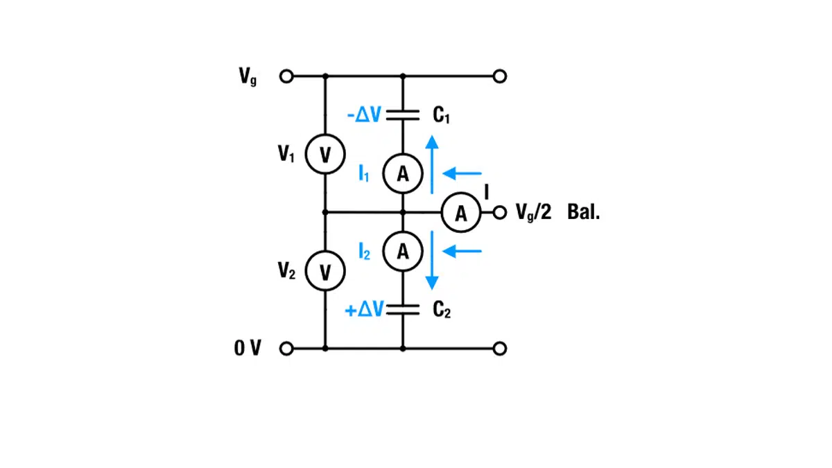
A useful first-order cell model consists of capacitance C, equivalent series resistance RESR, and a parallel leakage path. Real supercapacitors have additional distributed charge-storage and relaxation effects, so this simple model is most useful when its time scale and operating conditions are stated. Initially, neglect leakage and ESR and consider two initially discharged capacitors with capacitances C1 and C2. Figure 1 defines the two-cell stack and balancing-current paths. [1]
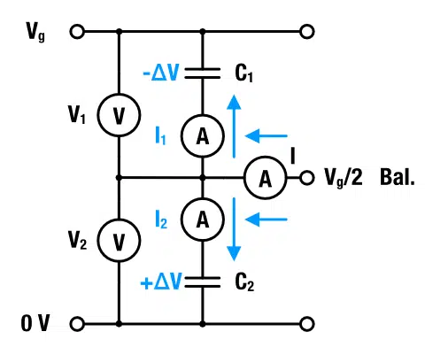
Before a balancing current enters the midpoint, the same series charging current supplies equal charge increments q to both ideal capacitors. With Vg as total stack voltage and V1 and V2 as individual cell voltages, their voltage division is given by Eq. (1).
The smaller capacitance therefore develops the larger voltage. Equal capacitances give equal cell voltages, but these equal voltages are not necessarily the rated voltage. Define Vt as the intended balanced cell voltage and Vr as the cell’s rated voltage. For a two-cell stack, the target is given by Eq. (2); the operating design must retain sufficient margin below the permitted cell voltage.
For C1 greater than C2, define ΔV as the positive deviation of either cell from Vt. The full cell-to-cell difference is 2ΔV, not ΔV. Equation (3) makes this distinction explicit.
Balancing changes the charge on the individual cells. The magnitudes of the required charge corrections are Δq1 for the lower-voltage cell and Δq2 for the higher-voltage cell. They are generally different when the capacitances differ, as shown in Eq. (4).
If those corrections occur over time Δt at constant average cell currents I1 and I2, Eq. (5) gives their magnitudes. One cell gains charge and the other loses charge. With the outer stack terminals held at fixed voltage, the midpoint driver must handle the sum of these current magnitudes, Imid. This is a midpoint-drive requirement, not a universal formula for the input current of an energy-transfer converter.
A longer stack can be reduced to two equivalent groups for some calculations. Such a reduction does not establish that every cell inside either group remains within its own voltage limit; individual cell monitoring or a justified cell-level protection strategy is still required.
Balancing Current and Balancing Time
Retain the original example of nominal capacitance Cr = 10 F with tolerance −10%/+30%. Choosing the two tolerance extremes gives C1 = 13 F and C2 = 9 F. At Vg = 5.4 V, Eqs. (1) and (3) give V1 = 2.209 V, V2 = 3.191 V and ΔV = 0.491 V. The cell-to-cell difference is approximately 0.982 V. This is the capacitance-only extreme for the specified tolerance and initial conditions, not a universal maximum imbalance. [1]
For correction in Δt = 1 s, Eq. (5) gives I1 = 6.382 A, I2 = 4.418 A and Imid = 10.8 A. If ΔV is first rounded to 0.5 V, the original illustrative values follow: 6.5 A, 4.5 A and 11 A. The difference is rounding rather than a different balancing principle.
For two cells of approximately equal nominal capacitance, Eq. (5) reduces to Eq. (6). Large capacitance and short balancing time can therefore require substantial midpoint current even when the voltage error appears modest.
Leakage, ESR and Operating Conditions
During prolonged voltage hold, leakage-current differences increasingly influence voltage division. An effective leakage resistance Riso can be defined at a specified voltage, temperature and conditioning time using Eq. (7), where Ileak is the measured leakage current. This is an operating-point approximation, not a constant material resistance. The original note discusses leakage measured after 72 h; use the actual cell datasheet’s conditioning and measurement procedure rather than treating that duration as universal. [1]
During current steps, the terminal voltage also contains an ESR-related contribution. This means a charging pulse can produce a terminal-voltage excursion that is not identical to the stored-capacitance voltage imbalance. Evaluate cell voltage during charging, at rest, and during discharge; do not infer the complete operating behaviour from one steady-state reading. [1][2]
Supercapacitor Balancing Methods and Strategies
Compare balancing methods by current capability, settling time, continuous loss, voltage accuracy, complexity and total installed cost. Also identify where the energy goes: dissipative shunts remove energy as heat, while suitable switching circuits transfer energy between cells. The labels “active” and “passive” alone do not describe either efficiency or protection capability. [1][2]
Passive Balancing with Resistors
Figure 2 shows equal resistors connected across the two cells. The resistors reduce the effect of unequal leakage paths and gradually move the midpoint towards half the stack voltage while the stack remains connected to its voltage source. They draw current continuously, including after balancing is complete. [1]
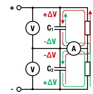
Resistor selection involves competing requirements: lower resistance increases correcting current and reduces balancing time, while higher resistance reduces standby consumption and self-discharge. Resistance matching and temperature tracking determine the divider accuracy; the original experiment used 1% resistors, but the required tolerance must follow the application’s voltage-error budget. [1]
The original application note proposes a starting value equal to one tenth of the effective leakage resistance. Equation (8) expresses that rule using rated cell voltage and the specified leakage current. It makes the resistor current approximately ten times that leakage current at Vr; it is a starting point, not proof of protection during charging or over temperature. [1]
Here Rb is the balancing resistance across each cell. For equal resistors, approximately voltage-independent leakage currents and a fixed total voltage, the residual cell-to-cell difference follows Eq. (9), where Ileak,1 and Ileak,2 are the two cell leakage currents. This approximation shows why the leakage mismatch, not only a nominal leakage value, matters.
Neglecting leakage and ESR, the midpoint time constant for two equal shunt resistors is τb = Rb(C1 + C2)/2. Define ΔV0 as the initial deviation and ΔVrem as the allowed remaining deviation. Equation (10) gives the corresponding settling time; for a 95% reduction of the initial error, the logarithmic factor is approximately three.
For approximately equal cells, this becomes t95 ≈ 3RbCr. A correcting current contribution proportional to ΔV/Rb should not be confused with the total current through a resistor, which is the complete cell voltage divided by Rb. Reducing Rb improves balancing speed but increases energy loss.
Table 1 preserves the original capacitance and leakage-current examples, using Vr = 2.7 V and recalculated rounded values. These are historical illustrative cell data, not a current component selection table. [1]
| Cell capacitance (F) | Leakage current (µA) | Balancing resistance (Ω) | Approximate 95% balancing time (h) |
|---|---|---|---|
| 3 | 8 | 33,750 | 84.4 |
| 5 | 12 | 22,500 | 93.8 |
| 7 | 20 | 13,500 | 78.8 |
| 10 | 30 | 9,000 | 75.0 |
| 15 | 60 | 4,500 | 56.3 |
| 25 | 68 | 3,971 | 82.7 |
| 50 | 105 | 2,571 | 107.1 |
These balancing times extend over several days. After the source is disconnected, an ideal cell discharging only through its balancing resistor follows Eq. (11), where V0 is its initial voltage and t is elapsed time. For the examples in Table 1, the resistor alone produces approximately 49–72% voltage loss in 24 h; there is no single common daily self-discharge percentage.
Pb in Eq. (11) is the instantaneous dissipation in one balancing resistor. Select resistance, power rating, voltage rating and temperature coefficient together. A resistor with resistance comparable to the cell ESR would impose an excessive continuous load and is not a practical route to very fast balancing.
Passive Balancing with Zener Diodes
A Zener diode connected across each cell provides a nonlinear shunt, as shown in Figure 3. Its current rises as the cell voltage approaches the diode’s operating region, potentially providing more correcting current than a high-value resistor while drawing less current at lower voltage. A nominal Zener voltage is specified at a particular test current, however; it is not an ideal clamp voltage. [1][3]
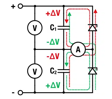
For the BZX79-B2V7 used in the original test, the checked datasheet specifies 2.65–2.75 V at a test current of 5 mA and a junction temperature of 25 °C. It also specifies substantial differential resistance and a temperature-dependent operating voltage. Consequently, selecting a nominal 2.7 V diode does not establish a sufficiently accurate protective limit for a 2.7 V cell. Allow margin for diode tolerance, current, temperature and charger overshoot. [3]
A diode can conduct in the forward direction if a cell is driven into reverse voltage, but that does not make unrestricted reverse operation acceptable. Any protective path must withstand the actual current and must keep the cell within the manufacturer’s permitted limits. Additional diodes across another balancing circuit should be assessed as part of the complete protection design rather than added by a universal rule.
The original note estimates a Zener balancing time by replacing the nonlinear shunt with an effective resistance. Equation (12) retains that historical approximation, where Pr is the diode power rating and fP is an assumed effective fraction of that rating. It is useful only as an illustrative estimate: the power rating is a thermal limit, not an operating current-voltage characteristic. [1][3]
The original example assumes fP = 0.1. A production design should instead use the relevant current-voltage and temperature data, or measured characteristics, and verify the transient behaviour. Do not use Eq. (12) to establish a guaranteed maximum cell voltage.
Self-Regulating Balancing with MOSFETs
Figure 4 shows a MOSFET-based balancing arrangement. Selected supercapacitor auto-balancing MOSFET arrays act as voltage-dependent shunts: their current rises strongly with the voltage applied in the specified connection. Their suitability depends on the device’s characterised current-voltage relationship, not simply on the presence of a MOSFET. [4]
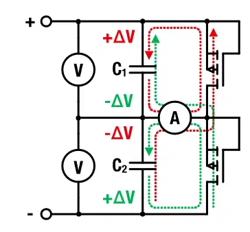
The ALD910022 used in the measurements is a dual auto-balancing MOSFET array. Its datasheet gives a nominal operating point of 2.20 V at 1 µA in the specified gate-drain-connected mode, with typical currents increasing to 100 µA at 2.42 V and 1 mA at 2.64 V. These operating points illustrate the nonlinear characteristic; they are not interchangeable with a guaranteed fixed-voltage clamp. [4]
Select the device characteristic so that its correcting current can accommodate the expected leakage mismatch before any cell reaches its permitted voltage. Include tolerance, temperature and power dissipation. A device intended primarily to balance leakage currents must not be assumed capable of bypassing the full charger current during rapid charging. The absolute maximum current rating is not the same as the available balancing current at a safe cell voltage. [4]
Terminology varies between publications: such circuits may be described as active or passive. In this article, the important distinction is that this arrangement is a self-regulating dissipative shunt, rather than an energy-transfer converter.
Active Midpoint Balancing with an Operational Amplifier
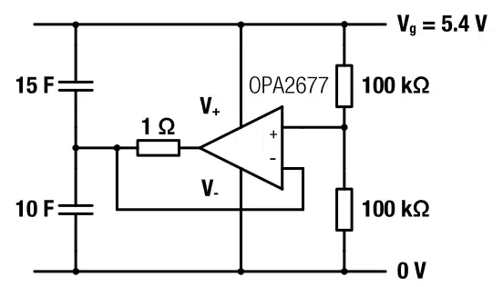
An operational amplifier can compare the actual midpoint voltage with a reference divider and source or sink correcting current, as illustrated in Figure 5. The resulting balancing speed depends on output-current capability, output headroom, current limiting, thermal design and loop stability. The amplifier’s supply current remains part of the standby energy budget. [1][5]
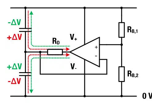
Choose the reference-divider resistance from input bias current, input offset, leakage, noise, resistor matching and the allowed voltage error. A generic rule based only on an assumed amplifier input resistance is inadequate. This is particularly important for the OPA2677 used in the experiment: it is a current-feedback amplifier, so its feedback-network requirements must also be respected. [5]
The output damping resistor RD helps isolate the amplifier from the capacitive load, but it also reduces available correcting current. Its value must be verified with the selected amplifier, feedback arrangement, cell ESR, wiring and operating conditions. Values that worked in the historical experiment are not universal stability limits.
This circuit is actively controlled but is not inherently an efficient energy-transfer topology. It can be appropriate when rapid voltage correction is more important than standby loss, provided the supply and thermal conditions are acceptable.
Active Balancing with DC-DC Conversion
A switching converter can move energy from a higher-voltage cell to a lower-voltage cell rather than dissipating the entire correction in a shunt. Figure 6 illustrates a converter-based balancing concept. Practical implementations differ in topology, current limits, activation thresholds, quiescent consumption and operation when the primary source is absent. [1][2]
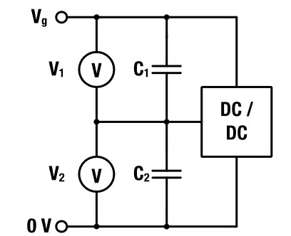
The LTC3128 combines a buck-boost charger with an inductor-based active charge balancer for a two-cell stack. Its datasheet describes transferring charge between the cells using the converter inductor, with balancing enabled under defined voltage and charging conditions. The charger’s input-current limit and the cell-to-cell balancing current are separate parameters. [2]
The LTC3351 is a different integrated backup-power architecture, supporting one to four series supercapacitors, charging and backup conversion, monitoring, balancing and per-cell protective shunts. Its presence of a bidirectional power converter does not mean that its cell balancing is the same inductor-based energy-transfer arrangement as the LTC3128. Review the balancing and protection circuits separately from the main charging converter. [6]
Integrated devices can reduce the number of separate charging, monitoring and protection functions, but they still require application-specific external components and qualification. Compare the complete circuit rather than the controller price alone. Low standby loss does not establish low charging loss, and neither value alone establishes conversion efficiency.
Coordinate the Balancer with the Charger
A balancing circuit cannot protect a cell indefinitely if the charger supplies more current than the available corrective path can accommodate. With a shunt balancer, the charger may need to reduce or interrupt charging as a cell approaches its upper limit. With an energy-transfer balancer, check the transfer-current capability and the conditions under which it operates. [2][6]
Cell overvoltage detection, stack regulation, current limiting and fault shutdown are related but distinct functions. Include startup with unequal cell voltages, loss of a midpoint connection and a damaged cell in the verification plan. A low steady-state voltage error is not proof of adequate fault protection.
Measurements
The following measurements are historical results from the Würth Elektronik application note, not new measurements of current products. They demonstrate the behaviour of five particular circuits with deliberately mismatched cells. Their timing and standby-loss values should not be treated as universal limits for the respective technologies. [1]
Measurement Setup and Comparison Limits
The voltage acquisition system used a CY8CKIT-059 PSoC development board with an Excel-based acquisition script. Jon-Izkue Rodriguez of Würth Elektronik developed the acquisition setup and script. The power supply was a Rohde & Schwarz HMP4040, and current measurements used a Gossen Metrawatt METRAHit ESPECIAL M252A multimeter. [1]
The test stack comprised a 10 F cell and a 15 F cell. The arithmetic mean capacitance was 12.5 F, while the series capacitance was 6 F. The general test conditions were a 5.4 V stack supply and a maximum charging current of 2 A; the LTC3128 board used a different stack-voltage setting, described below. [1]
Combining different nominal capacitances was an experimental choice, not a recommended production configuration. Without balancing, the ideal capacitance-only division at 5.4 V would place 3.24 V across the 10 F cell and 2.16 V across the 15 F cell: deviations of ±0.54 V from the 2.7 V midpoint. This deliberately large mismatch made the behaviour reproducible and exposed the circuits to demanding conditions.
The original note reports severe lifetime reduction during overvoltage exposure, although catastrophic failure was not observed in its tested samples. That observation must not be interpreted as a safe operating allowance. Production designs must remain within the selected cells’ specified operating limits. [1]
For retention measurements, the primary source was disconnected after charging while the balancing circuit remained connected to the cells. Measurements continued over 24 h. The original discussion uses “long-term” to mean several days, but a 24 h voltage trace does not establish a guaranteed multi-day hold-up time under load. [1]
For a reproducible comparison, define the remaining voltage error used to declare balancing complete, the initial cell voltages, stack target, charging-current profile, temperature and measurement loading. Also identify every supply rail included in a loss measurement. Input-side consumption, current drawn from the stored-energy stack and heat dissipated during charging are different quantities.
Resistor, 1 kΩ Passive Balancing
The resistor experiment used a 1 kΩ, 1%, 0.6 W resistor across each cell, following Figure 2. Figure 7 shows the reported approach to equal voltage over approximately 600 min. The resistance was selected to favour balancing speed over energy retention. [1]
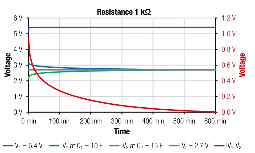
Using Eq. (10), the 10 F and 15 F cells give τb = 12,500 s and t95 = 624.1 min. The three-time-constant approximation gives 625 min. This is consistent with the reported approximately 600 min settling interval, although a numerical comparison requires a common completion criterion.
After 12 h, the reported maintaining current was 2.8 mA at 5.4 V, corresponding to 15.12 mW. For comparison, the two ideal 1 kΩ resistors at 2.7 V each dissipate 14.58 mW in total, or 7.29 mW per resistor. The small difference includes other current paths and measurement conditions. A large resistor power rating does not reduce the energy consumed by the chosen resistance. [1]
To estimate retention, first define Cstack as the series capacitance. If total losses can be represented by an effective resistance Req = Vg,0/Iloss,0, the voltage half-life follows Eq. (13), where Vg,0 and Iloss,0 are the initial stack voltage and loss current. This is an equivalent-resistance approximation, not a constant-current discharge formula.
For Cstack = 6 F, Vg,0 = 5.4 V and Iloss,0 = 2.8 mA, Eq. (13) gives 133.7 min. The reported measurement in Figure 8 was approximately 130 min. Because the two individual RbC time constants differ, the isolated stack is not exactly a single exponential; the estimate is useful here but should not be treated as an exact model. [1]
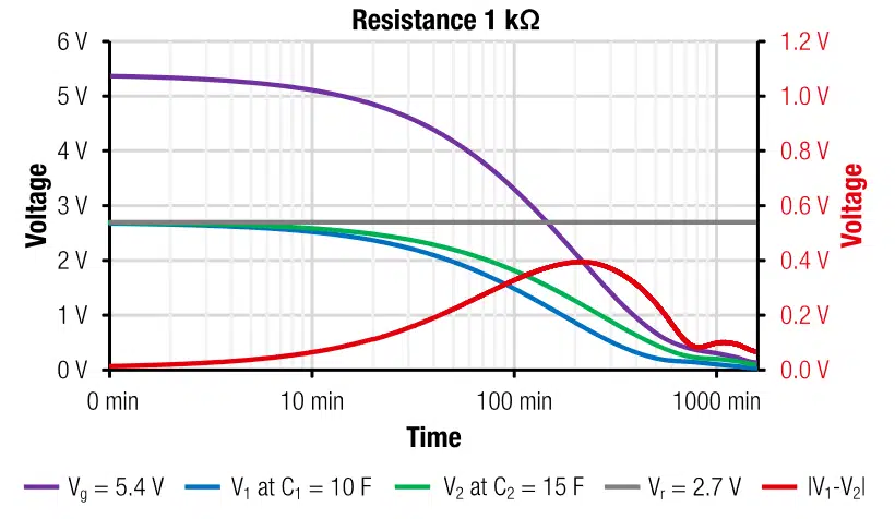
A voltage half-life of approximately two hours can be acceptable for a short backup duty, but it is not evidence of good multi-day storage. Increasing the resistance improves retention at the expense of balancing speed and leakage-mismatch correction. Select the compromise against the actual load and minimum operating voltage.
Zener Diode Passive Balancing
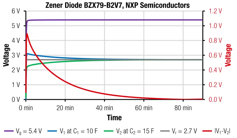
The Zener experiment used BZX79-B2V7 voltage-regulator diodes, identified as NXP devices in the original work. The checked datasheet is now hosted by Nexperia. Figure 9 shows reported balancing in approximately 80 min. [1][3]
Recalculating Eq. (12) with Vr = 2.7 V, Pr = 0.5 W, Cr = 12.5 F and fP = 0.1 gives the result in Eq. (14). This is approximately 91 min, not the 70 min stated in the original calculation. The difference between the approximate model and the measured 80 min is unsurprising for a nonlinear shunt.
The reported maintaining current after 12 h was 5 mA at 5.4 V, giving 27 mW. The datasheet’s 20 µA reverse-current limit at 1 V is specified for an individual diode under stated test conditions; it is not a measured stack leakage current at the operating voltage. Likewise, the 500 mW power limit depends on the specified thermal mounting conditions. [1][3]
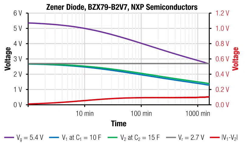
The original note also illustrates a retention estimate by multiplying 20 µA by an assumed factor fI = 10 and using the equivalent-resistance approach. Equation (15) retains that calculation with explicit assumptions. IR,1V denotes the diode reverse-current value at 1 V; fI is an illustrative adjustment, not a characterised physical constant. [1][3]
Replacing ln(2) with 0.7 gives approximately 1,890 min, explaining the original rounded value of approximately 1,900 min. Figure 10 shows the reported retention behaviour, but this empirical approximation does not establish a guaranteed half-life or loaded backup duration. Use measured current-voltage behaviour or a direct retention test over the required voltage range. [1]
MOSFET Self-Regulating Balancing
The MOSFET arrangement used an Advanced Linear Devices SABMB2 test board populated with the ALD910022. Figure 11 shows reported balancing in approximately 300 min. The maintaining current after 12 h was 1.5 mA at 5.4 V, equivalent to 8.1 mW. This is lower than the 27 mW reported for the tested Zener circuit, not approximately the same loss. [1]
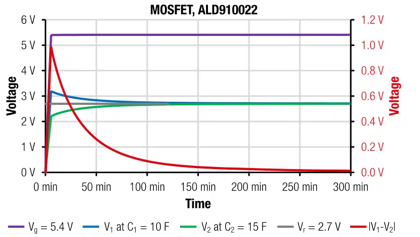
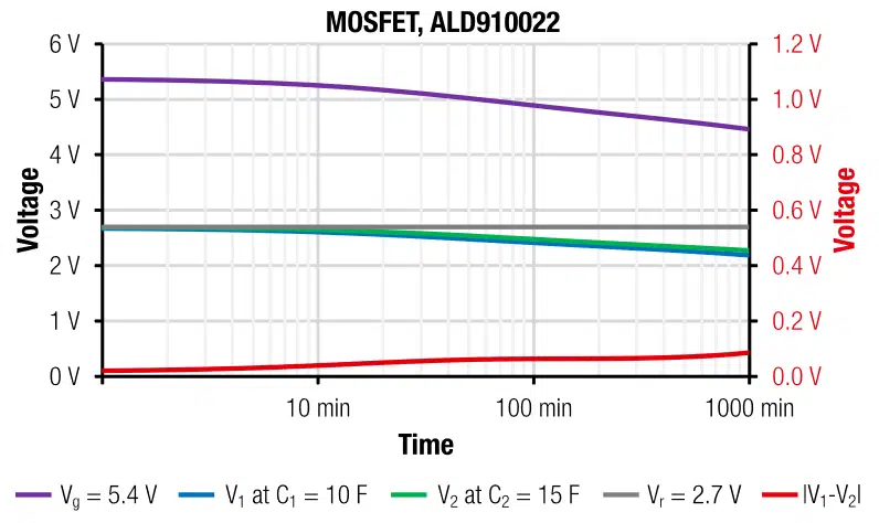
Figure 12 shows the reported total stack voltage falling from approximately 5.4 V to approximately 4 V after 24 h. The original authors compared this behaviour with Würth Elektronik retention data and concluded that the balancing circuit did not substantially increase self-discharge in their example. The result supports consideration for low-loss standby use, but a controlled comparison with the same cells and the required load is necessary to establish application performance. [1]
Amplifier Active Balancing
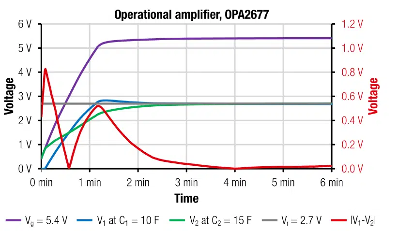
The amplifier experiment used the Texas Instruments OPA2677 in the arrangement shown in Figure 13. Its datasheet’s headline 500 mA output capability depends on supply and test conditions and should not be read as a guaranteed continuous balancing current at every stack voltage. Check the relevant output-current, output-swing and thermal specifications for the implemented circuit. [1][5]
The reported stack balanced within the charging interval, approximately 3 min, as shown in Figure 14. Reducing the damping resistor from 1 Ω to 0.4 Ω shortened the reported time to approximately 2 min but introduced decaying oscillation. The authors selected 1 Ω as the better compromise for that setup. Neither value is a general stability recommendation for other amplifiers or layouts. [1]
The reported maintaining current after 12 h was 50 mA at 5.4 V, giving 270 mW. The particular amplifier circuit therefore consumed much more standby power than the tested resistor, Zener and MOSFET arrangements. This is a result for the implemented circuit, not a universal power requirement of all amplifier-based balancers. [1]
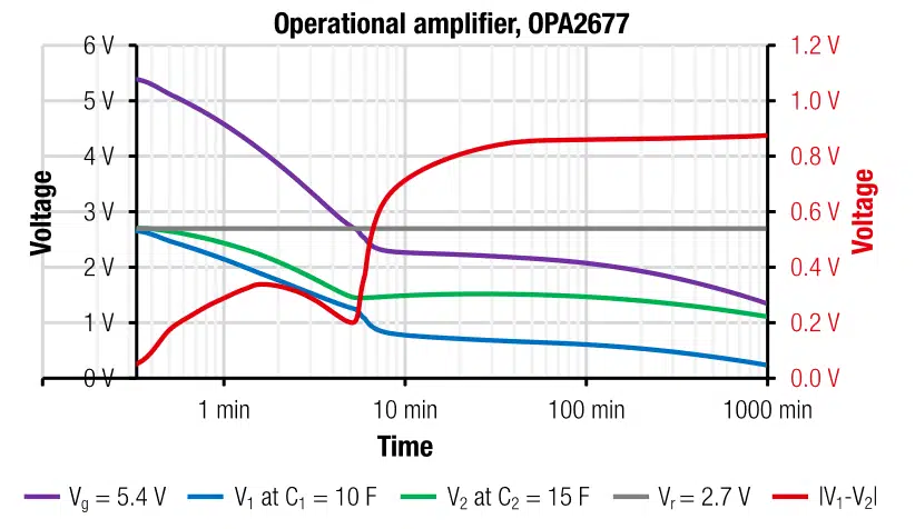
Figure 15 shows a reported voltage half-life of approximately 5 min. That makes this implementation unattractive for long unattended retention. Its useful demonstration is rapid midpoint control; a production design would need an acceptable standby-current budget, defined low-voltage behaviour and verified stability. The current drawn after source removal need not equal the maintaining current measured with the source present. [1]
Active Balancing with the LTC3128 Board
The DC1887A evaluation board used the Analog Devices LTC3128 buck-boost charger and balancer. In this experiment, the total stack target was 4.2 V and the supply voltage was reported as 5.5 V. The 4.2 V value describes the complete stack, not each cell. The reported balancing interval was approximately 1.5 min. [1]
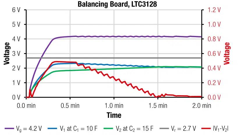
The note reports a 0.1 mA maintaining-current figure and an approximately 0.5 mW power estimate. That estimate is of the expected magnitude, but its stated voltage multiplier is not consistent with the separately described 5.5 V supply and 4.2 V stack. Treat it as a reported low-power operating-point result, not a complete independently established board-loss measurement or a conversion-efficiency measurement. [1]
The LTC3128 datasheet specifies separate current consumption from the input and output, with different values during sleep, balancing and shutdown. This illustrates why a single measured current cannot represent every operating state or supply path. [2]
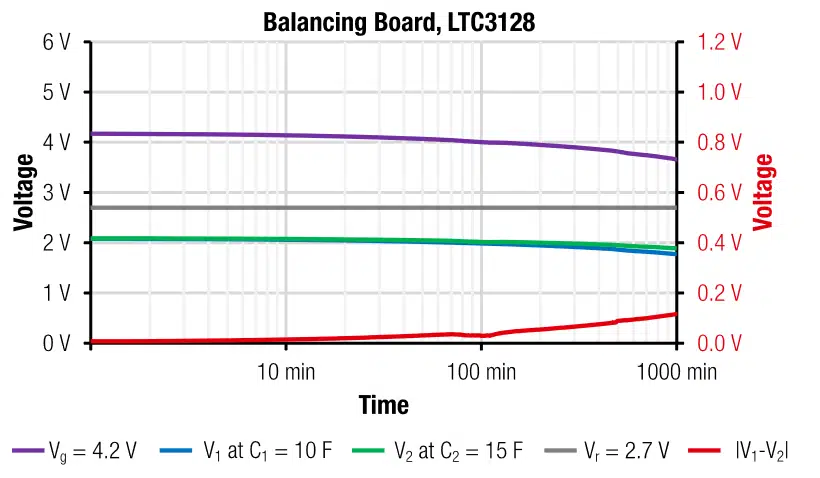
Figure 17 shows the reported total stack voltage declining from 4.2 V to approximately 3.4 V after 24 h. The result supports considering this architecture for low-loss backup storage, but it does not by itself establish multi-day loaded operation. Its lower starting voltage and different charging conditions also prevent a direct like-for-like speed or energy comparison with the 5.4 V experiments. [1]
Summary – What Is the Best Supercapacitor Balancing Method?
There is no single best balancing method independent of the application. Table 2 summarises the historical measurements while keeping their operating conditions and limitations visible. Balancing speed, standby consumption and installed cost must be evaluated together with voltage accuracy, protection and the intended charge-discharge duty.
| Tested arrangement | Reported balancing interval | Reported maintaining-power result | Selection interpretation |
|---|---|---|---|
| 1 kΩ resistors | Approximately 600 min | 15.12 mW at 5.4 V | Simple and inexpensive, but continuous discharge is significant. |
| BZX79-B2V7 Zener diodes | Approximately 80 min | 27 mW at 5.4 V | Nonlinear shunt; voltage margin and temperature require careful checking. |
| ALD910022 MOSFET arrangement | Approximately 300 min | 8.1 mW at 5.4 V | Useful for leakage balancing when the selected current-voltage characteristic fits the cells. |
| OPA2677 amplifier arrangement | Approximately 3 min with the selected damping arrangement | 270 mW at 5.4 V | Fast midpoint correction, with high standby consumption in this implementation. |
| DC1887A with LTC3128 | Approximately 1.5 min at a 4.2 V stack target | Approximately 0.5 mW reported; measurement boundary requires clarification | Integrated charging and energy-transfer balancing; different test conditions limit direct comparison. |
Resistors are appropriate when simplicity and low component cost dominate and the continuous load is acceptable. Zener diodes can provide a stronger voltage-dependent shunt, but low-voltage characteristics and tolerances limit clamp precision. Selected MOSFET arrays can reduce the added current at lower cell voltage, but their correction capability must match the leakage distribution.
Amplifier circuits can provide rapid correction, but their supply current and stability deserve particular attention. Switching energy-transfer circuits can combine balancing with efficient charging and low standby draw, although they add control, layout and component-selection requirements. A production cost comparison should include external components, qualification, firmware where applicable, assembly and lifecycle availability rather than reproduce historical relative-price labels.
Design and Selection Checklist
Choose the circuit from a worst-case operating model, then verify it on representative hardware. The checklist applies to EDLC backup and power-buffer stacks; safety-critical systems and other storage chemistries require additional application-specific requirements.
- Define the duty: required backup time, maximum load, minimum usable stack voltage, recharge time, pulse current, ambient range and expected service life.
- Compare cell datasheets: rated voltage, permitted operating conditions, capacitance tolerance, ESR and its measurement method, leakage-current conditioning, temperature behaviour, endurance and end-of-life limits.
- Calculate voltage distribution for minimum and maximum capacitance, unequal starting voltages and leakage mismatch. Include resistor tolerance, sensing error, temperature drift and ESR-related voltage excursions.
- Check corrective current at the permitted cell voltage, not only a device’s headline or absolute maximum current. Verify resistor or shunt dissipation and thermal derating.
- Coordinate charging and balancing: verify when balancing starts, whether it operates during charging or after regulation, and how the charger responds when a cell reaches its upper limit.
- Budget all standby paths: cell leakage, balancing elements, voltage dividers, controller supply current, indicators, monitoring electronics and any current flowing back into an unpowered source.
- For a catalog module, obtain the internal balancing topology, protection limits, terminal definitions, retention conditions and qualification evidence. Do not infer these from nominal stack voltage alone.
- For a custom assembly, specify the approved cell and balancer combinations, wiring and sensing arrangement, thermal design, production screening, traceability and replacement policy. Initial cell matching does not eliminate aging-related divergence.
- Qualify abnormal operation: unequal initial charge, excessive leakage, cell short circuit, open sensing or balancing connections, source interruption, restart and excessive discharge. Establish appropriate current limiting, protective shutdown and safe discharge provisions.
- Confirm applicable end-product safety and environmental requirements with the responsible qualification team. Component ratings and an evaluation-board demonstration do not establish compliance of the finished equipment.
Measure Usable Energy, Not Only Voltage Half-Life
Voltage half-life is a convenient retention descriptor, but it is not energy half-life or backup duration. For approximately constant capacitance, Eq. (16) gives stored energy E and the ideal energy Eusable available between initial voltage Vstart and cutoff voltage Vcutoff. Converter losses, ESR, balancing consumption and the actual load reduce the energy delivered to the application.
For an unchanged capacitance, reducing voltage to one half leaves one quarter of the initial stored energy. A useful validation therefore records individual cell voltages, stack voltage, load current and time until the actual system cutoff, rather than declaring success from a no-load voltage trace alone.
Practical Verification Sequence
Condition the cells according to their datasheets, then test representative capacitance and leakage combinations over the required temperature range. Record initial conditions and use the same completion threshold when comparing balancing times. Confirm the effect of the measurement equipment’s input current, particularly when assessing low-leakage cells.
Use suitable differential or isolated measurement methods for elevated cell nodes; an earth-referenced instrument connection must not short a stack node. Check startup and transient behaviour separately from long-duration retention, and repeat the loaded backup test with the intended charger, converter, wiring and protection circuits connected.
Conclusion
Supercapacitor balancing must address both dynamic capacitance mismatch and long-duration leakage mismatch without consuming an unacceptable share of the stored energy. The original measurements illustrate the trade-off: simple shunts can settle slowly, a high-current amplifier can settle quickly but consume substantial standby power, and an integrated energy-transfer circuit can offer a different combination of charging, balancing and retention.
Select the architecture by the required correction current, permitted cell-voltage error, charging behaviour, standby budget and fault response. Then qualify the complete stack under its actual load and temperature conditions. Neither a balanced midpoint nor a low reported standby-power value alone establishes a reliable backup-power design.
FAQ
Series-connected cells do not necessarily divide the total voltage equally. Capacitance differences affect voltage during charging, while leakage-current differences affect voltage during prolonged voltage hold. Balancing limits this divergence, but its current capability and accuracy must suit the application. A safe total stack voltage alone does not guarantee that every individual cell remains within its permitted operating voltage.
Select the resistance from leakage mismatch, allowed cell-voltage error, required settling time and acceptable continuous loss. The historical rule of one tenth of effective leakage resistance is only a starting point. Check resistor matching, temperature coefficient, power rating and self-discharge, then verify charging transients. A resistor that corrects steady-state leakage mismatch may still be too slow for rapid charging.
A nominal 2.7 V Zener is not an ideal 2.7 V clamp. Its specified voltage applies at a stated test current and temperature, and actual voltage depends on tolerance, current and temperature. The complete shunt and charger arrangement must keep the cell within its permitted operating limit. Matching the nominal diode voltage to the cell rating does not establish adequate protection.
Selected MOSFET arrays provide a strongly voltage-dependent shunt current across the cells in their specified connection. Their correcting current increases as operating voltage rises. Selection must use the characterised current-voltage relationship, leakage mismatch, temperature and available voltage margin. These devices do not automatically provide energy transfer, and a leakage-balancing device should not be assumed capable of bypassing the full charging current.
No. Active describes control or circuit implementation, not necessarily the energy path. An operational amplifier can regulate the midpoint quickly while consuming significant supply current, and a controlled shunt still dissipates energy. An appropriate switching balancer can transfer energy between cells. Compare the complete circuit during charging, standby and source-disconnected operation rather than relying on the active or passive label.
The best choice depends on the required retention time, load, cutoff voltage, recharge duty and fault requirements. Continuous resistor loss may be unacceptable for long unattended storage, while selected nonlinear shunts or low-standby integrated circuits can offer alternatives. Measure the full assembly under the intended load and temperature conditions. A no-load voltage trace does not establish guaranteed loaded backup duration.
Balancing reduces voltage differences between cells during specified operating conditions. Overvoltage protection prevents a cell from exceeding its permitted voltage, including when available balancing current is insufficient or a fault occurs. The functions must be coordinated with the charger. A well-balanced stack during normal operation does not prove that charging will stop safely after a cell or sensing connection fails.
How to Select and Verify a Supercapacitor Balancing Circuit
Select a balancing architecture and verify the complete EDLC stack under its intended operating and fault conditions.
- Define the operating requirements
Record stack voltage, permitted cell voltage, load, cutoff voltage, backup duration, recharge time and temperature range. Obtain the cell capacitance, ESR and leakage specifications with their measurement conditions.
- Calculate the worst-case imbalance
Calculate charging voltage division using capacitance extremes and unequal initial charge. Evaluate leakage mismatch during voltage hold and include sensing error, component tolerance, temperature drift and ESR-related terminal-voltage excursions.
- Select and coordinate the balancing method
Compare correcting current, settling time, standby consumption and thermal requirements. Check the actual current-voltage behaviour of nonlinear shunts. Confirm how the charger reduces or stops charging when a cell reaches its upper limit.
- Test charging and voltage retention
Measure every cell during startup, charging, voltage hold and source disconnection. Use consistent initial conditions and completion thresholds. Check measurement loading and all supply-current paths, then measure backup duration with the intended load and cutoff.
- Qualify faults and document production limits
Verify temperature extremes, unequal starting voltages, damaged cells and interrupted sensing or balancing connections. Document approved components, protection settings, thermal limits, production checks and replacement requirements before releasing the assembly.
Further Reading
The following articles provide background on cell construction, alternative balancing implementations and complete backup-power systems.
- Supercapacitors — background on construction, electrical behaviour, leakage and measurement.
- Evaluation of Active Balancing Circuits for Supercapacitors — a separate experimental study of monitored multi-cell stacks and controlled balancing.
- WE Backup Your Application – A Real-Life Supercapacitor Backup Solution — system-level context for charging, conversion and industrial backup power.
- MOSFET-Based Automatic Supercapacitor Balancing — further explanation of voltage-dependent MOSFET leakage balancing.
References
References [1]–[6] support the theory, original experimental results and device-specific descriptions. Datasheet operating conditions and limits take precedence over simplified illustrative models.
- René Kalbitz, Würth Elektronik, Keep the Balance – Balancing of Supercapacitors, application note ANP090a, Würth Elektronik, 2021.
- Analog Devices / Linear Technology, LTC3128: 3 A Monolithic Buck-Boost Supercapacitor Charger and Balancer with Accurate Input Current Limit, datasheet 3128f, Analog Devices, undated document version.
- NXP Semiconductors / Nexperia, BZX79 Series: Voltage Regulator Diodes, product datasheet, NXP Semiconductors, 2002; hosted by Nexperia.
- Advanced Linear Devices, ALD810022/ALD910022: Quad/Dual Supercapacitor Auto Balancing MOSFET Array, datasheet, Advanced Linear Devices, undated document version.
- Texas Instruments, OPA2677: Dual, Wideband, High Output Current Operational Amplifier, datasheet SBOS126I, Texas Instruments, revised 2008.
- Analog Devices, LTC3351: Hot Swappable Supercapacitor Charger, Backup Controller and System Monitor, datasheet, revision B, Analog Devices, undated document version.