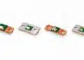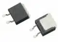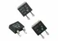


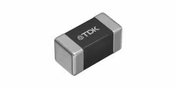





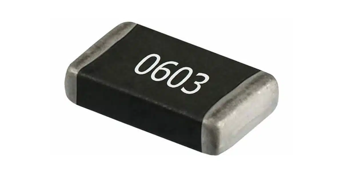
SMD chip resistors are fixed resistors designed for direct surface mounting on printed circuit boards. They are the default resistor format in modern electronic equipment because they support automated assembly, compact layouts and short electrical interconnections.
However, a chip resistor is not defined only by its nominal resistance: technology, package geometry, tolerance, temperature coefficient, working voltage, power dissipation, pulse capability and PCB layout can all determine whether the design remains accurate and reliable over its intended lifetime.
This guide explains the main SMD resistor technologies and package formats, then provides practical guidance for selecting, rating and mounting chip resistors in general-purpose, precision, power-conversion, RF, automotive and industrial applications. For high-frequency circuits, short interconnections are beneficial, but actual RF performance also depends on the resistor geometry, PCB pads, surrounding copper and supplier frequency-characterization data.
Key Takeaways
- SMD resistors enable miniaturization and short interconnections; high-frequency performance depends on resistor construction, package geometry and PCB layout.
- Different types include thick film, thin film, and metal foil, each with specific applications and characteristics.
- Thick film resistors are cost-effective for general-purpose use, while thin film resistors cater to precision applications.
- Key considerations for selection include resistance, tolerance, power rating, and thermal performance.
- Proper layout and assembly practices enhance reliability and performance of SMD resistors.
SMD Resistor Package Sizes and Codes
SMD chip resistors are commonly identified by a four-digit package code. The same physical size may be expressed in imperial units of hundredths of an inch or in metric units of tenths of a millimetre. For example, an imperial 0402 package is approximately 1.0 mm × 0.5 mm and is therefore called 1005 in the metric naming system.
Always verify the dimensional drawing in the chosen manufacturer datasheet. Package names are useful shorthand, but actual body dimensions, terminal dimensions, resistance range, voltage rating and power rating may differ between resistor series.
| Imperial code | Metric code | Nominal body size | Typical use |
|---|---|---|---|
| 0201 | 0603 | 0.60 mm × 0.30 mm | Extreme miniaturization; mobile and high-density electronics |
| 0402 | 1005 | 1.00 mm × 0.50 mm | High-density general-purpose designs |
| 0603 | 1608 | 1.60 mm × 0.80 mm | General-purpose digital and analog circuitry |
| 0805 | 2012 | 2.00 mm × 1.25 mm | General-purpose designs with more power or voltage margin |
| 1206 | 3216 | 3.20 mm × 1.60 mm | Higher-power, higher-voltage and pulse-loaded positions |
| 1210 | 3225 | 3.20 mm × 2.50 mm | Power, current-sense and pulse applications |
| 2010 | 5025 | 5.00 mm × 2.50 mm | Higher continuous power and surge capability |
| 2512 | 6432 | 6.30 mm × 3.20 mm | Power dissipation, shunts and high-energy pulse duties |
Reverse-geometry packages use the same dimensional naming principle, but their long and short axes are exchanged. A 0612 reverse-geometry resistor, for example, has the same nominal body outline as a conventional 1206 part but places its terminals on the long sides. This can reduce current-path inductance and improve heat transfer into the PCB when the manufacturer’s recommended footprint is used.
Resistance Marking and Identification
Larger chip resistors are often marked with their resistance code, whereas smaller packages are commonly unmarked because there is insufficient surface area. The marking identifies the nominal resistance only; it does not identify tolerance, TCR, power rating, voltage rating, technology or qualification level. Those characteristics must be obtained from the bill of materials and manufacturer part number.
| Marking system | Example | Nominal resistance | Explanation |
|---|---|---|---|
| 3-digit code | 472 | 4.7 kOhm | First two digits are significant; third digit is the power-of-ten multiplier |
| 4-digit code | 1001 | 10 kOhm | First three digits are significant; fourth digit is the multiplier |
| R notation | 4R7 | 4.7 Ohm | The letter R acts as the decimal point |
| Zero-ohm link | 0 or 000 | 0 Ohm nominal | Specified as a jumper with a maximum resistance and a current rating |
| EIA-96 code | 01C | 10 kOhm | Two digits select an E96 base value; the letter specifies the multiplier |
For failure analysis, repair or reverse engineering, do not rely on a printed code alone. Parallel circuit paths, board contamination, damaged solder joints and in-circuit measurement errors can make the measured resistance differ from the nominal value.
Overview of SMD Chip Resistor Types
SMD resistor technology extends far beyond basic thick-film chips. The most appropriate resistor family is determined by the electrical function and operating environment: general-purpose biasing requires a different construction from precision feedback, current sensing, repetitive surge handling or RF termination. Thick-film resistors dominate high-volume general-purpose applications, while thin-film, metal-foil, metal-strip and specialized resistor families address tighter accuracy, lower noise, higher pulse energy or lower parasitic inductance.
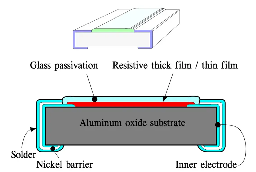
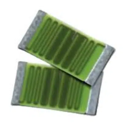
Most rectangular chip resistors use an alumina ceramic substrate with metal end terminations. A resistive layer is then formed by screen-printing and firing a thick-film paste, depositing a thin metallic film, bonding a foil element or welding a metal-strip element. Protective glass and polymer overcoats provide environmental and mechanical protection. The construction details, terminal system and trimming method vary by technology and manufacturer.
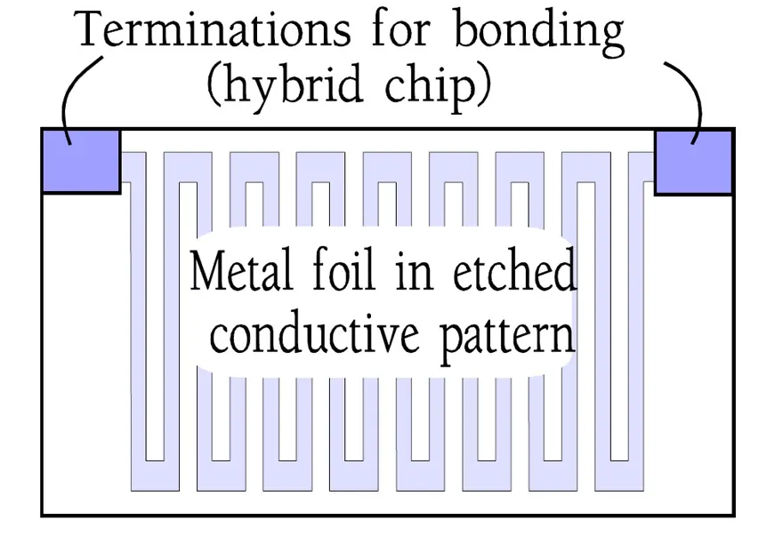
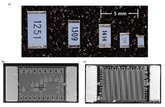
Laser trimming is widely used to set resistance accurately, particularly for thick-film resistors. The resulting trim geometry can influence current-density distribution during short overloads. For pulse- or surge-critical positions, select a resistor series explicitly qualified for the required pulse waveform, peak voltage, energy and repetition rate; do not infer capability from the presence or absence of a visible trim pattern.
Thick Film Chip Resistors
Thick film chips are the standard choice for general‑purpose signal paths, pull‑ups and pull‑downs, bias networks and timing components. They offer a very wide resistance range from low ohmic values up to tens of megaohms, with good cost efficiency and robust manufacturing. Typical tolerances are 1–5% and TCR in the 50–200 ppm/°C range, which is sufficient for most non‑precision applications.
Thin Film Chip Resistors
Thin film resistors target precision analog and measurement applications where accuracy, low noise and stability are important. They typically provide tolerances from 0.1–1% and TCR as low as 10–25 ppm/°C, but with more limited power and resistance range compared to thick film. Thin film is widely used in instrumentation amplifiers, ADC/DAC interfaces, precision voltage dividers and feedback networks in high‑performance op‑amp circuits.
Metal Foil Chip Resistors
Metal foil resistors represent the high‑end class for ultra‑stable, low‑noise and very low TCR performance. They exhibit excellent long‑term drift and minimal resistance change with temperature, load and time, making them suitable for metrology, reference circuits and demanding laboratory instruments. Their drawback is higher cost and typically larger footprint compared with mainstream thick and thin film technologies.
Current Sense (Shunt) Chip Resistors
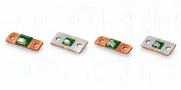
Current sense resistors are optimized to measure high currents with low power loss, usually in the milliohm range. They use specialized constructions such as metal strips or optimized thick‑film geometries and often offer Kelvin‑sense terminals for accurate low‑ohmic measurements. Typical applications are battery management, DC‑DC converters, motor drives and power distribution paths where precise current monitoring and efficiency are important.
Current-Sense Resistor Layout and Accuracy
For milliohm current-sense resistors, PCB copper resistance and thermal gradients can create errors comparable to, or larger than, the resistor tolerance. Use a true Kelvin connection where accuracy matters: route separate sense traces from the resistor terminals to the measurement amplifier input, outside the high-current path.
- Place the current-sense amplifier close to the shunt where practical, while keeping sensitive sense traces away from switching nodes.
- Use symmetric copper around the shunt terminals to reduce temperature-gradient-induced offset and unequal heat spreading.
- Check the shunt TCR over the full operating temperature range, not only its 25 °C resistance tolerance.
- For fast-switching converters, verify the shunt inductance and the amplifier’s input filtering, common-mode range and transient response.
- For high current, use dedicated metal-strip or four-terminal shunts rather than treating a standard low-ohmic chip resistor as an interchangeable substitute.
Power Chip Resistors
Power chip resistors are designed to dissipate significantly higher power than standard chips in similar or only slightly larger footprints. This is achieved by optimized materials, larger terminations and improved thermal coupling to the PCB. They are used in power supplies, snubber networks, bleeder resistors and other locations where continuous or frequent high dissipation occurs.
Reverse‑Geometry and Wide‑Terminal Resistors
Reverse‑geometry parts swap length and width (for example 1225 instead of 2512) to improve thermal performance and lower inductance. Wide‑terminal designs couple heat more efficiently into the PCB and can provide better power handling and reduced ESL than standard shapes. These components are attractive in high‑power density designs and high‑frequency circuits, but they require careful footprint design and assembly process control.
The design benefits are in these fields:
- lower ESL = lower parasitic and higher frequency range
- better thermal conduction into the PCB = potentially higher power capability for comparable footprint area, depending on the specific package, test board and manufacturer rating conditions
- higher mechanical strength = higher vibration and flex stress robustness
- less thermal stress as differences in the coefficient of expansion between substrate and chip decreases in significance with shorter distances between terminations.
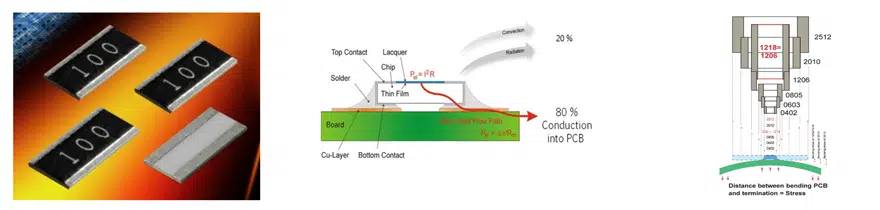
The downside of the design, considering the high manufacturing price is now almost identical, is a significantly more difficult PCB cleaning process in narrow and long gaps between the termination pads.
Jumpers and Zero‑Ohm Links
Zero‑ohm chip resistors act as configurable links, net jumpers or simple cross‑overs on densely routed boards. They are specified both by maximum resistance and maximum continuous current, which must be respected for reliable use. Designers often use them for configuration options, rework flexibility and to replace wire links in automated assembly.
Integrated and Buried Resistors
Resistor networks and arrays integrate multiple resistors into a single package, reducing placement count and improving matching. In addition, some PCB technologies support embedded resistive layers that implement buried resistors directly inside the board stack‑up. These approaches are attractive in high‑density, high‑volume products where space, performance and BoM optimization are critical.
Comparison of SMD Resistor Technologies
The table below is intended as an initial technology-selection guide. The ranges are indicative only: the available resistance range, tolerance, TCR, rated power, working voltage and stability must always be confirmed for the exact package and resistor series.
| Technology or family | Strengths | Typical limitations | Typical applications |
|---|---|---|---|
| General-purpose thick film | Low cost, wide resistance range, broad package availability | Higher noise and drift than precision technologies; standard versions may have limited pulse capability | Pull-ups, pull-downs, biasing, timing, logic and non-critical analog circuits |
| Thin film | Tight tolerance, low TCR, low noise, good stability | Usually higher cost and narrower resistance/power availability than general-purpose thick film | Precision analog, feedback networks, ADC/DAC interfaces, instrumentation |
| Metal foil | Very low TCR, excellent long-term stability and low noise | Higher cost, often larger package and more limited availability | Metrology, references, laboratory instruments and high-end precision systems |
| Metal strip or shunt | Milliohm resistance range, high current capability, low inductance options | Requires careful Kelvin layout and thermal-gradient management | Battery management, DC-DC converters, motor drives and power distribution |
| Pulse-proof or anti-surge | Improved overload, inrush and pulse handling | Pulse performance is waveform- and repetition-dependent | Snubbers, inrush paths, discharge circuits and protection functions |
| High-voltage resistor | Higher working-voltage capability and controlled voltage stress | Power, creepage, clearance and overload requirements still apply | Voltage dividers, mains-related sensing and high-impedance measurement |
| RF or low-ESL resistor | Controlled high-frequency behavior; lower parasitic inductance in suitable geometries | Requires frequency data and PCB-specific validation | RF matching, attenuators, transmission-line termination and fast-edge damping |
| Network or array | Reduced placement count; potential ratio and thermal tracking advantages | Power must be derated per element; crosstalk and matching specifications vary | Pull-up arrays, termination arrays and matched divider networks |
Electrical Characteristics and Selection Criteria
Beyond resistance and package size, the main performance drivers for SMD chip resistors are tolerance, temperature coefficient, voltage and power rating, noise and long‑term stability. A structured view of these parameters helps to select the right device early in the design.
Resistance Range and Tolerance
Different technologies cover different resistance ranges and typical tolerance classes. Thick film offers the broadest range with standard tolerances of 1–5%, while thin film and foil focus on tighter tolerance but with somewhat restricted resistance span. For most digital biasing or pull‑up functions 1–5% is sufficient, whereas precision analog paths may require 0.1–0.5% parts or matched networks.
Temperature Coefficient of Resistance (TCR)
TCR expresses how much the resistance changes with temperature in ppm/°C. Common classes for thick film are around 100–200 ppm/°C, while thin film can reach 10–25 ppm/°C and foil even lower. When the operating temperature range is wide, TCR can dominate the overall error budget and justify the cost of a better technology.
Precision Parameters Beyond Tolerance and TCR
Initial tolerance and TCR do not fully define accuracy in a precision circuit. The designer should also consider long-term drift, load-life stability, humidity stability, voltage coefficient of resistance (VCR), power coefficient of resistance (PCR), excess noise and thermal electromotive force where very low-level signals are involved.
- VCR describes resistance change with applied voltage and can be significant in high-value divider resistors.
- PCR describes resistance change caused by self-heating under dissipation, even at constant ambient temperature.
- Ratio tracking is often more important than absolute tolerance in gain-setting dividers and differential signal paths.
- Long-term drift should be evaluated under the relevant combination of load, temperature, humidity and time.
- Thermal EMF can become important in low-level DC measurement circuits where dissimilar metals or temperature gradients produce unwanted thermoelectric voltages.
Where resistor ratio accuracy is critical, a matched resistor network can outperform separately mounted components because its elements share more closely matched processing, temperature conditions and mechanical environment. Verify ratio tolerance and ratio TCR directly from the network datasheet.
Power Rating and Derating
The stated power rating of an SMD resistor is not a universal installed-board capability. It is measured under defined conditions, including a specified test board and reference temperature. IEC 60115-8:2023 introduced a reference-temperature concept for determining rated power, which makes it especially important to compare supplier ratings only in the context of their stated conditions.
Use the manufacturer derating curve for the exact resistor series, then assess the actual application: maximum ambient temperature, adjacent heat sources, copper area, thermal vias, airflow, enclosure temperature, pulse duty cycle and required service life. Using 50–60% of nominal rated power can be a conservative internal design rule in demanding applications, but it is not a universal requirement and must not replace thermal validation.
For a first calculation, resistor dissipation can be determined as P = I²R or P = V²/R. The result must then be checked against the applicable continuous-power derating curve, maximum working voltage, limiting element voltage and any pulse-load limit.
Operating Voltage and Limiting Element Voltage
Each chip size has a specified maximum continuous working voltage and overload voltage. At high resistance values, the limiting element voltage may restrict safe operation even if the power rating appears sufficient. Designers must check both power and voltage limits, especially in mains‑related circuits, surge‑exposed nodes and high‑impedance dividers.
High-Voltage and Safety Considerations
A resistor working-voltage rating is an electrical component rating; it is not, by itself, a safety-insulation rating for an assembled product. In mains-connected, high-voltage or safety-related designs, verify the complete system requirement: creepage and clearance on the PCB, pollution degree, altitude, coating condition, expected surge events, overload behavior, flame resistance and the applicable end-product safety standard.
For high-voltage dividers, multiple resistors in series may be used to distribute voltage and dissipation. Their values, voltage coefficients, parasitic capacitances and physical placement should be arranged so that voltage sharing remains acceptable under steady-state, transient and contaminated-board conditions. Use high-voltage-qualified or pulse-qualified resistor series where the application requires them.
Noise and Stability
Resistor noise behavior differs between technologies, with thick film generally noisier than thin film and foil. Long‑term stability is also strongly technology‑dependent and can be affected by load, humidity and temperature cycling. Precision applications benefit from low‑noise, low‑drift technologies, while mass‑market digital circuits usually tolerate higher noise and drift.
Power Handling, Pulse and Surge Capability
After the basic power and voltage ratings have been selected, verify how the resistor behaves in the installed application. Continuous dissipation depends on board thermal conditions, while pulses and surges are governed by waveform, peak voltage, energy, duration, repetition rate and the resistor series construction. Use the manufacturer’s derating curve and pulse-load graph for the exact part number.
Continuous Power and Thermal Design
Continuous dissipation is limited by the maximum permissible temperature of the resistive element and terminations. Standard data sheets define power ratings on reference test boards that may be more optimistic than dense real‑world layouts. Enlarging copper areas, using thermal vias and avoiding hotspots around the part significantly improves temperature margins.
Derating and Temperature Rise
Manufacturers provide derating curves that reduce allowable power above a given ambient temperature. For demanding applications, it is good practice to apply additional design derating on top of those curves to achieve the desired lifetime and reliability. Thermal simulations or simple temperature measurements on prototypes help to validate assumptions before release.
Pulse and Surge Ratings
Short pulses and surges are limited by instantaneous film temperature and current density rather than average power. Many series include dedicated pulse‑proof versions with optimized film geometry, terminations and substrates. For inrush, load dump, ESD or protection tasks, the designer should always consult pulse load and energy withstand graphs in the data sheet.
Influence of Laser Trimming
Laser trimming can create local current-density concentrations in some thick-film designs, which may influence overload behaviour. For pulse-critical positions, select a resistor series using the manufacturer’s specified pulse-load, overload-voltage and repetition-rate data; do not use trim geometry alone as a qualification criterion.
High‑Frequency Behaviour and Parasitics
At RF and with very fast digital edges, SMD chip resistors behave as a combination of resistance, inductance and capacitance. Package geometry, pad layout and surrounding copper all influence this high‑frequency behavior.
Parasitic Elements (ESL and ESR)
Each chip resistor exhibits an equivalent series inductance (ESL) due to current paths through the terminations. Long, narrow terminations and large loop areas increase ESL and can limit performance at high frequencies. Reverse‑geometry and wide‑terminal parts reduce loop area and thus ESL, offering better behavior for high‑speed or RF signals.
Capacitive Coupling
Chip resistors also show parasitic capacitance to the ground plane and to neighboring tracks. This can be critical for very high‑value resistors, high‑impedance nodes and HF matching networks. Careful layout with controlled clearances and minimized overlapping copper under sensitive components helps to reduce these effects.
Layout Guidelines for High‑Frequency Use
- Keep connections short and minimize loop area around the resistor.
- Place components close to active devices and transitions.
- Use symmetric placement and identical packages in differential or matched networks.
When frequencies or edge rates become high enough that generic thick‑film parts no longer meet performance, dedicated RF chip resistors with specified S‑parameter behavior should be considered.
Typical Applications of SMD Chip Resistors
SMD chip resistors are used across virtually all electronic equipment, from low‑cost consumer products to high‑reliability automotive and industrial systems. Understanding the application context helps to choose the right technology, size and rating for each position in the circuit.
Signal Conditioning and Bias Networks
In analog and mixed‑signal designs, SMD resistors set gains, offsets and bias points in amplifiers, filters and sensor interfaces. Thin film types are often preferred where low noise, tight tolerance and good long‑term stability are required, for example in instrumentation amplifiers, ADC/DAC front‑ends and precision voltage dividers. For less demanding biasing or pull‑up functions, standard thick film chips usually offer sufficient accuracy at lower cost.
Digital Pull‑Ups, Pull‑Downs and Terminations
Digital I/O lines typically use SMD resistors as pull‑ups, pull‑downs and line terminations. The main requirements here are appropriate resistance, adequate voltage rating and sufficient power margin, while tolerance and TCR are often of secondary importance. Thick film resistors in standard chip sizes dominate this area thanks to their low cost and wide value range.
Power Management and Current Sensing
In power conversion and distribution, SMD resistors serve as current sense elements, inrush limiters, bleeders and snubbers. Dedicated current‑sense chips or shunt resistors with low resistance, Kelvin terminals and high pulse capability are used to measure battery, motor or converter currents accurately and efficiently. Power chip resistors and pulse‑proof series are chosen where high continuous dissipation or repetitive surge loading is expected, for example in start‑up circuits, RC snubbers or discharge paths.
RF, High‑Speed and Impedance Control
At RF and high data rates, chip resistors appear in matching networks, attenuators, terminations and damping elements in transmission lines. Here the parasitic inductance and capacitance of the package and layout become critical, so reverse‑geometry, wide‑terminal or dedicated RF resistor series are often used. Careful placement, short connections and symmetric layouts help maintain controlled impedance and signal integrity.
Automotive, Industrial and Harsh Environments
Automotive ECUs, industrial control units and other harsh‑environment systems place stringent demands on resistor robustness and reliability. Components must withstand wide temperature ranges, thermal cycling, vibration and in some cases sulfur‑rich atmospheres. Designers therefore often select AEC‑Q200‑qualified thick or thin film series, sulfur‑resistant terminations and conservative derating for power and voltage stress.
Reliability, Assembly and Layout Guidelines
Many practical failures involve solder joints, terminations or mechanical damage rather than pure resistive element defects. Assembly, PCB design and environmental conditions therefore play a central role in the reliability of SMD chip resistors.
Many field failures associated with SMD resistors originate in solder joints, end terminations, PCB flexure or the local thermal environment rather than in the resistive element itself. Larger packages and long, narrow components are generally more sensitive to board bending and differential expansion because the distance between their terminations is greater.
Typical Failure Mechanisms
- Thermal-cycling fatigue: repeated temperature change can fatigue solder joints and termination interfaces.
- Board-flex cracking: depanelization, connector insertion, handling or enclosure stress can crack the ceramic body or solder joint.
- Overload damage: continuous overheating, high element voltage or pulse energy beyond the approved curve can cause resistance drift, open circuit or catastrophic damage.
- Sulfur-related termination corrosion: sulfur-containing atmospheres can attack susceptible termination systems and eventually create high resistance or open circuits.
- Assembly defects: uneven pads, incorrect stencil apertures, inadequate reflow control, voiding and excessive solder volume can create uneven stress or poor joints.
Do not use a single arbitrary temperature-cycle count as a generic quality criterion. Required endurance depends on the resistor construction, package size, environmental category, customer specification and applicable qualification standard. Automotive designs commonly use AEC-Q200-qualified components, but qualification should be treated as evidence of defined stress testing, not as a substitute for application-specific design margins.
Assembly and Footprint Recommendations
Footprints should follow recognized standards and manufacturer recommendations to ensure balanced solder fillets and avoid tombstoning. Oversized pads and excessive solder volumes can increase mechanical stress and the risk of cracking or voids. Solder stencil design (aperture size, thickness, paste type) must match the chosen package sizes and assembly process capability.
Component Orientation and Board Design
Component orientation can influence both thermal gradients and mechanical robustness. For high‑power resistors, it is often preferable to follow the manufacturer’s recommended land pattern and ensure balanced copper around both terminals. Evaluate actual board temperatures where the resistor dissipates significant power. For current‑sense parts, orientation that minimizes current path length and ensures symmetrical copper on both sides of the component improves measurement accuracy and thermal balance.
Board layout should avoid placing critical resistors in areas prone to bending, such as near slots, cut‑outs or connectors. Adding copper “heat‑spreaders” and thermal vias under high‑power parts reduces local temperature rise and improves lifetime.
Quick Layout Checklist
Before releasing a PCB with critical SMD resistors, check at least the following points:
- Power dissipation on each resistor under worst‑case conditions, including derating.
- Voltage across high‑value resistors vs limiting element voltage rating.
- Pad size, stencil design and symmetry to avoid tombstoning and cracking.
- Position relative to board edges, slots and mechanical stress points.
- Thermal environment, copper area and potential hotspots in the surrounding layout.
Standards and Qualification
Resistor datasheets commonly reference standards that define terminology, test methods, environmental categories or qualification requirements. Standards do not remove the need to validate the exact component in its intended circuit and PCB environment, but they provide a common basis for comparing declared performance.
- IEC 60115-1: generic specification for fixed resistors used in electronic equipment, including common terms, inspection procedures and test methods.
- IEC 60115-8:2023: sectional specification for fixed surface-mount resistors. It covers preferred ratings, characteristics and test requirements for this resistor category.
- AEC-Q200 Rev. E: stress-test qualification for passive components intended for automotive use. AEC-Q200 qualification must be verified for the exact supplier series and temperature grade.
- IPC-7351: land-pattern design guidance for surface-mounted components, including chip resistors. Manufacturer-recommended footprints should take priority where they differ from generic library assumptions.
For safety-critical, automotive, medical, aerospace, rail or other regulated applications, also review customer specifications and system-level standards. A qualified resistor does not automatically demonstrate compliance of the complete assembly.
Conclusion
SMD chip resistors are not interchangeable commodities when precision, power, pulse energy, high voltage, high frequency or harsh environmental conditions matter. A reliable choice starts with the electrical function, then considers technology, package, resistance accuracy, temperature behavior, voltage stress, continuous and transient dissipation, PCB layout and assembly environment.
For general-purpose functions, standard thick-film resistors are often appropriate and cost-effective. For critical functions, select the resistor family from verified application data: thin film or foil for precision, metal-strip shunts for current measurement, pulse-proof series for surge duty, high-voltage series for divider networks and RF-characterized parts for frequency-sensitive circuits.
Before release, review each high-power, high-voltage, precision, current-sense and safety-related resistor against its exact datasheet, derating curve, pulse graph and recommended footprint. This targeted review prevents most avoidable resistor failures and improves lifetime performance of the finished assembly.
SMD Chip and MELF Resistor Characteristics
Conventional rectangular chip resistors and cylindrical MELF resistors are both surface-mount components, but their geometry, available technologies and assembly behaviour differ. The values and statements below are indicative only: actual resistance range, tolerance, TCR, power rating, working voltage, pulse performance and qualification depend on the exact manufacturer series and package size.
| Characteristic | Rectangular SMD chip resistor | MELF resistor | Design implication |
|---|---|---|---|
| Body geometry | Rectangular ceramic body with end terminations | Cylindrical body with metalized end faces | Chip resistors are widely used for dense automated assembly; MELF parts may require placement equipment configured to prevent component rolling. |
| Available technologies | Thick film, thin film, metal foil, metal strip/shunt, high-voltage, anti-surge, RF and wide-terminal variants | Commonly metal film, carbon film, metal glaze and precision thin-film variants | Select the technology and qualified series first; body style alone does not define accuracy, reliability or pulse capability. |
| Typical resistance range | From milliohm shunts to tens or hundreds of megaohms, depending on technology | Typically from sub-ohm values to several megaohms, depending on film type and size | Both styles cover broad ranges; verify the exact required value and tolerance for the selected series. |
| Initial tolerance | Typically ±1% to ±5% for general-purpose thick film; tighter grades available in thin film, foil and networks | Typically ±1% to ±5%; precision MELF versions can reach ±0.1% or tighter | Use tolerance together with TCR, VCR/PCR, ratio tracking and long-term drift when circuit accuracy matters. |
| TCR and stability | Strongly technology-dependent: general-purpose thick film is typically less stable than thin film or foil | Metal-film and precision MELF series can provide low TCR and good long-term stability | For precision or high-voltage divider functions, compare published drift, humidity, load-life and voltage-coefficient data. |
| Continuous power dissipation | Wide range, from very low power in miniature packages to several watts in power-chip, metal-strip or wide-terminal series | Often favourable for the occupied board area in larger MELF formats | Use the manufacturer’s rated-power conditions and derating curve; installed-board copper area and ambient temperature are decisive. |
| Pulse and surge performance | Ranges from limited standard thick-film capability to high performance in dedicated anti-surge, pulse-proof, high-voltage and metal-strip series | Often strong, particularly for qualified carbon-film or metal-film MELF pulse-load series | Compare the correct pulse waveform, voltage, energy, duration and repetition rate. Never compare pulse capability by package appearance alone. |
| Working voltage | Package- and series-dependent; dedicated high-voltage chip resistors are available | Often favourable in larger cylindrical packages; high-voltage series are available | Check maximum working voltage and limiting element voltage independently of the power rating. |
| High-frequency behaviour | Small chips, reverse geometry and wide terminals can offer low inductance; dedicated RF series may provide frequency data | Leadless cylindrical geometry can be suitable for many applications, but RF behaviour is series- and footprint-dependent | For RF or fast switching, use impedance or S-parameter data and validate the installed PCB layout. |
| Mechanical and environmental robustness | Good when footprint, solder process and board-flex controls are correct; long rectangular packages can be more sensitive to PCB bending | Cylindrical construction can offer strong resistance to thermal cycling, humidity and pulse-induced stress in qualified series | For harsh environments, verify AEC-Q200, sulfur resistance, humidity performance, temperature grade and board-flex data for the exact part. |
| Assembly considerations | Excellent compatibility with standard high-speed pick-and-place and reflow processes | Requires appropriate placement and reflow process control to avoid rolling or positional movement | Use the supplier’s recommended land pattern, stencil aperture and assembly guidance for the selected package. |
| Typical best-fit applications | General electronics, precision analog, current sensing, dense digital layouts, RF, high power and automotive designs | High pulse load, high stability, demanding environmental conditions, high-voltage dividers and selected precision applications | Choose according to verified electrical, thermal, environmental and manufacturing requirements rather than package preference. |
Note: This table is a technology-selection guide, not a component specification. Confirm all final ratings from the current manufacturer datasheet, derating curve, pulse-load graph, qualification report and recommended PCB footprint.
Note: Last technically reviewed: September 2026. Ratings and qualification status should always be verified against the latest manufacturer documentation.
References
The standards and resources below provide the primary basis for resistor terminology, qualification, footprint design and final component verification. Access to full standards documents may require purchase or organizational subscription.
- IEC 60115-8:2023 — Fixed surface-mount resistors. Sectional specification for fixed resistors designed for surface mounting; consult the current edition for formal requirements and rating conditions.
- IEC 60115-1 — Fixed resistors for use in electronic equipment. Generic fixed-resistor specification covering terminology, inspection procedures and test methods.
- AEC-Q200 Rev. E — Stress Test Qualification for Passive Components. Automotive Electronics Council qualification document and related supporting requirements.
- IPC-7351 — Generic Requirements for Surface Mount Design and Land Pattern Standard. Land-pattern design guidance for surface-mounted electronic components.
- Passive Components Blog: IEC 60115-8 Revision 3 and Reference Temperature for Rated Power. Editorial explanation of the revised power-rating approach for SMD resistors.
- Manufacturer datasheets, recommended land patterns, derating curves, pulse-load graphs and qualification reports for the exact resistor series and package selected.
Technical review note: Resistance range, tolerance, TCR, working voltage, rated power, pulse capability and qualification status are series- and package-specific. Confirm the final selection against the latest manufacturer documentation and applicable system-level requirements.
Further Reading
The following Passive Components Blog articles provide deeper coverage of resistor construction, technology selection, pulse capability, qualification and application-specific design considerations.
- What Is a Resistor? — fundamentals of resistance, resistor functions and basic circuit use.
- Resistor Types and Construction Fundamentals — construction methods, resistor families and technology-related performance differences.
- Thin Film and Metal Film Resistors — detailed comparison of thin-film, metal-film, metal-foil, thick-film and carbon resistor technologies.
- Resistor Technology Selection and Benchmark Guidelines — structured method for selecting resistor technology against precision, pulse, power and environmental requirements.
- Resistors Pulse Load and Derating Design Guide — practical procedures for continuous power, voltage, surge-energy and pulse-load verification.
- Resistor Technologies Pulse Load Comparison — comparison of material and geometry factors that influence resistor pulse performance.
- SMD Surface Mount Chip Resistor Selection Guide — additional background on thick-film and thin-film chip resistor deposition methods.
- IEC 60115-8 Revision 3 Enhances SMD Resistor Safety by Introducing a New Concept of Reference Temperature for Rated Power — implications of the IEC 60115-8:2023 revision for SMD resistor power ratings.
- 2025 Thick and Thin Film Resistor Networks Environment Overview — resistor network technologies, applications and supply-chain context.
FAQ: SMD Chip Resistors
SMD chip resistors are fixed surface-mount resistive components designed for automated PCB assembly. They enable compact layouts and short electrical paths; their usable high-frequency performance depends on resistor construction, package geometry, land pattern and surrounding PCB layout.
The main SMD resistor types are thick film, thin film, metal foil, current sense (shunt), power chip, reverse-geometry or wide-terminal parts, jumpers, and integrated or buried resistor networks.
Thick film resistors are best for cost-sensitive, general-purpose functions such as pull-ups, pull-downs and bias networks, while thin film resistors are preferred in precision analog, measurement and low-noise applications.
Selection should consider resistance value, tolerance, TCR, power rating, limiting element voltage, pulse and surge capability, noise and long-term stability, as well as the thermal and mechanical conditions on the PCB.
Power rating is limited by the maximum allowable temperature of the resistive film and terminations, which depends on chip size, PCB copper area, airflow and derating above the reference ambient temperature.
Reverse-geometry and wide-terminal resistors can reduce current-path inductance, improve thermal coupling into the PCB and improve resistance to board-flex stress. The actual benefit depends on the package, resistor series, land pattern and manufacturer rating conditions.
At high frequencies, SMD resistors exhibit parasitic inductance and capacitance. Package geometry, pad layout, surrounding copper and return-current path influence the resulting impedance. Use supplier frequency-response or S-parameter data when RF or fast-edge performance is critical.
Typical failures include cracked solder joints from thermal cycling, ceramic body cracks from PCB bending or handling, and sulfur-induced corrosion of terminations in harsh environments.
Automotive ECUs, industrial control, power management and other harsh-environment designs often use AEC‑Q200-qualified or sulfur-resistant SMD resistors combined with conservative derating for voltage and power.
Using proper footprints, balanced pads, suitable stencil design, good component orientation, generous copper for heat spreading and avoiding flex zones under critical resistors significantly improves reliability.
They are package-size codes. Imperial codes describe nominal dimensions in hundredths of an inch, while metric codes describe nominal dimensions in tenths of a millimetre. For example, imperial 0402 is approximately 1.0 mm × 0.5 mm and corresponds to metric 1005.
Larger chip resistors may use three-digit, four-digit, R notation or EIA-96 codes. Smaller packages are often unmarked. The printed marking identifies nominal resistance only and should not be used as proof of tolerance, TCR, power rating or resistor technology.
Limiting element voltage is the maximum continuous voltage that may be applied across the resistive element. It can limit high-value SMD resistors before their nominal power rating is reached, so both voltage and power ratings must be checked.
No. A 50% or 60% limit can be a conservative internal design practice, but the correct allowable dissipation depends on the manufacturer derating curve, ambient temperature, PCB thermal design, neighbouring heat sources, pulse duty cycle and required lifetime.
Use Kelvin sensing when milliohm resistance, high current or measurement accuracy makes PCB trace resistance significant. Separate sense traces should connect directly to the resistor terminals and avoid carrying load current.
Yes. Series connection can distribute voltage and power, but each resistor must remain within its own continuous voltage, power and pulse limits. In high-voltage dividers, also consider resistance tolerance, voltage coefficient, parasitic capacitance, PCB creepage and clearance, contamination and transient voltage sharing.
A sulfur-resistant resistor uses a construction and termination system designed to withstand sulfur-containing environments more effectively than standard products. Select it when the equipment may encounter sulfur-bearing gases or materials, and verify the manufacturer’s stated test method, conditions and qualification for the exact resistor series.
A resistor array can reduce placement count and PCB area, and matched resistor networks can provide improved ratio and thermal tracking. However, check the permitted dissipation per element, total package dissipation, isolation arrangement, voltage rating and the manufacturer’s matching specifications.
How to select SMD chip resistors for reliable electronic designs
- Identify the function of each resistor in the circuit
Review the schematic and classify each SMD resistor as a signal path element, bias or pull-up/pull-down, current sense, snubber, bleeder, termination, or RF/high-speed component.
- Choose an appropriate resistor technology
Use thick film for general-purpose and digital functions, thin film or foil for precision and low-noise analog paths, dedicated current-sense chips for high currents, and RF-optimized or reverse-geometry types for high-frequency applications.
- Define resistance, tolerance and TCR requirements
Set the nominal resistance from circuit calculations, then assign suitable tolerance and TCR ranges based on accuracy needs and operating temperature span; use tighter values for measurement and reference circuits.
- Check power dissipation and apply derating
Calculate worst-case power dissipation for each resistor, compare it with the datasheet rating and derating curve for the exact series, then validate the installed-board temperature. Additional design margin may be appropriate for demanding lifetime, ambient-temperature or pulse-load conditions, but it should not be applied as a universal fixed percentage.
- Verify voltage, pulse and surge limits
Ensure that the maximum steady-state voltage across each resistor is below its limiting element voltage and that any pulses, surges or inrush events stay within the specified pulse load and energy withstand capabilities.
- Account for parasitics in high-frequency or fast-switching circuits
For RF, high-speed digital and sensitive analog nodes, consider the package ESL and stray capacitance; select suitable geometries, keep connections short and use symmetric layouts or dedicated RF resistor series when needed.
- Design footprints and layout for reliability
Follow recommended land patterns, stencil designs and pad symmetry, avoid placing high-stress resistors near board edges or slots, and use adequate copper and thermal vias to manage temperature and mechanical stress.
- Review critical resistors before release
Before finalizing the design, systematically check high-power, high-voltage, precision and safety-related SMD resistors against all electrical, thermal and mechanical criteria to ensure sufficient margins and reliability.
- Confirm the approved manufacturer part number and production controls
Confirm the exact package, technology, tolerance, TCR, power and voltage rating, pulse qualification, temperature grade, termination option and AEC-Q200 status where required. Release the manufacturer-recommended footprint, stencil guidance and approved alternates together with the bill of materials so that purchasing and production do not substitute a visually similar but electrically unsuitable part.