




Alessandro Paghi, Farbod Abazar and colleagues from the University of Pisa, with contributors from Scuola Normale Superiore, CNR Nanosciences and CISUP in Pisa, report a method for directly manufacturing three-dimensional copper microinductors on electronic chips.
The open-access research article was published in Nature Communications on 8 September 2026.
Introduction
Inductors are indispensable in radio-frequency integrated circuits, where they support impedance matching, filtering, resonant networks and other signal-conditioning functions. Yet conventional on-chip inductors are typically implemented as planar metal spirals, which consume substantial silicon area and can become an important constraint on chip size, performance and cost.
The problem becomes more severe as RF circuits are miniaturised. Increasing the inductance of a planar spiral generally requires more turns or a larger occupied area, while substrate-related losses and parasitic capacitances can limit high-frequency operation. The result is a persistent trade-off between inductance, quality factor, footprint and usable frequency range.
The authors address this limitation by moving the inductor into the third dimension. Their approach creates freestanding copper microsolenoids directly on chip contact pads, allowing the winding volume to extend above the silicon rather than across it. For broader background on inductor operation and practical loss mechanisms, see Inductance, Impedance, Q Factor and DCR Losses.
Key points
- The study demonstrates maskless three-dimensional electrodeposition of copper microinductors directly on chip contact pads.
- The printed components are freestanding microsolenoids that use vertical space above the chip surface rather than a large planar silicon footprint.
- The fabrication method can be applied after standard chip production, without requiring changes to the underlying integrated-circuit design.
- Several copper microsolenoid geometries were fabricated on test chips and electrically characterised.
- The demonstrated devices provided inductance in the nanohenry range.
- Measured quality factors reached values of up to 18.
- The microinductors retained inductive behaviour up to 15 GHz.
- Electrical measurements agreed with electromagnetic simulations.
- The work proposes a scalable route towards smaller RF integrated circuits and potentially lower manufacturing costs.
- The approach may be relevant wherever conventional planar inductors dominate chip area or restrict circuit integration.
Extended summary
RF integrated circuits rely on inductors, but these components do not scale as easily as transistors or many active devices. A conventional integrated inductor is commonly formed as a planar spiral in the chip metallisation stack. This geometry is compatible with standard fabrication, but it requires area on the silicon die. As the coil becomes larger or gains additional turns, it competes directly with active circuitry for valuable chip surface.
Planar geometries also expose the inductor to losses associated with the substrate and parasitic effects caused by closely spaced conductors. At high frequency, these non-ideal effects can reduce quality factor and eventually cause the component to stop behaving primarily as an inductor. This makes compact, efficient on-chip magnetic components an important technical challenge for RF electronics.
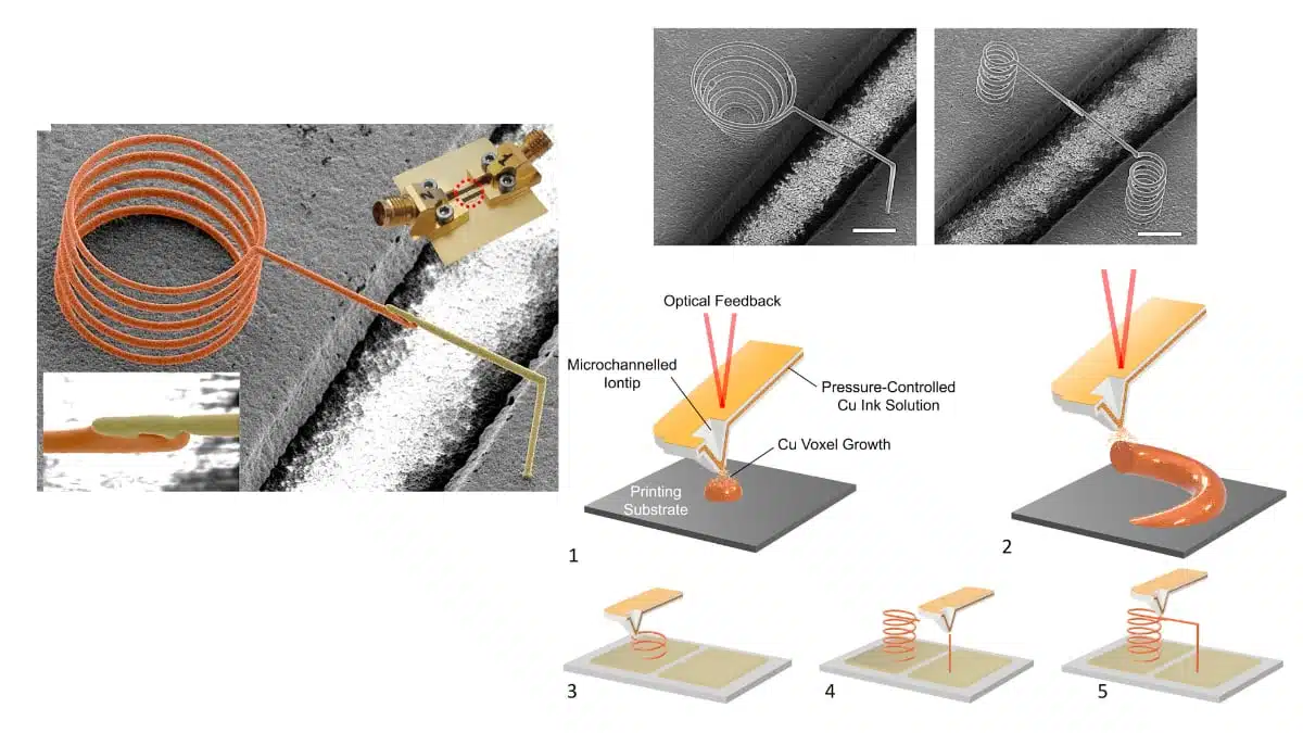
The reported work takes a different physical approach: rather than forming a coil in the chip plane, the researchers build a three-dimensional copper solenoid above the chip. The microinductor is fabricated directly on chip contact pads by high-precision electrodeposition. In effect, the process turns the available volume over the die into a functional magnetic structure, reducing the dependence of inductance on the two-dimensional silicon area beneath it.
The copper structures are freestanding microsolenoids. Their geometry permits a coil-like magnetic field configuration while using a compact pad-level base connection. This is particularly important because inductance depends not only on conductor length and number of turns, but also on the geometry of the magnetic field created by the winding. Moving turns vertically above the surface can therefore offer a different area-efficiency path than extending a planar spiral laterally.
The process is described as maskless, meaning the 3D metal structures are formed without introducing a dedicated lithographic mask sequence for each coil geometry. The authors position this as a post-fabrication integration method: it can be applied after conventional chip fabrication and does not require redesigning the underlying circuit. Such separation between IC fabrication and magnetic-component addition could make the concept attractive for specialised RF chips or heterogeneous integration flows.
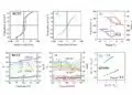
The researchers fabricated copper microsolenoids with different geometries on test chips. Their electrical behaviour was characterised over a wide frequency range and compared with electromagnetic simulations. The agreement between measurements and simulations supports the physical interpretation of the devices and indicates that their RF response can be predicted with established electromagnetic modelling methods.
The measured devices achieved inductance values in the nanohenry range, which is directly relevant to many RF matching, filtering and resonant applications. They reached quality factors as high as 18. In an RF inductor, quality factor is a practical measure of the balance between useful reactance and losses; higher values are generally desirable because they reduce loss in resonant and impedance-transformation networks.
The printed microsolenoids remained inductive up to 15 GHz. This result is particularly significant because parasitic capacitance, conductor resistance and substrate interaction often constrain conventional integrated inductors as frequency rises. The reported frequency performance suggests that the printed structures can serve in RF regimes where compact passive integration is demanding.
The work does not claim that three-dimensional printing automatically replaces every planar inductor technology. Instead, it demonstrates a fabrication and integration platform that changes the central geometry constraint. By decoupling inductance from planar silicon real estate, the process may enable RF circuit designers to reclaim die area while retaining a locally integrated magnetic function.
The concept also illustrates a broader trend in advanced electronics packaging: performance-critical passive structures increasingly move beyond the traditional two-dimensional metallisation stack. Similar thinking is relevant to the development of miniaturised inductive devices and integrated magnetic technologies, including Researchers Expand Microchip Capability with New 3D Inductor Technology.
Conclusion
This research demonstrates that copper microinductors can be additively manufactured as three-dimensional microsolenoids directly on chip contact pads. The devices provide nanohenry-scale inductance, quality factors up to 18 and inductive behaviour extending to 15 GHz.
The main contribution is not only the measured RF performance, but the manufacturing concept: a maskless, post-fabrication method that shifts inductive structures above the silicon surface. This could reduce the area penalty traditionally associated with on-chip RF inductors.
Further work will need to establish how the approach performs across larger wafer-scale or package-scale manufacturing flows, how it integrates with specific RF circuit architectures, and how reliability, process repeatability and application-level cost compare with established integrated-inductor technologies.
Further reading
- Inductance, Impedance, Q Factor and DCR Losses
- What Is an Inductor?
- One Turn Inductors Explained
- Inductance, AC Inductors and DC Inductors Explained in Video
Source
This article is based on the open-access scientific publication in Nature Communications. Engineers should consult the current original article, supplementary information and applicable manufacturing documentation before component qualification or design release.