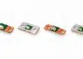







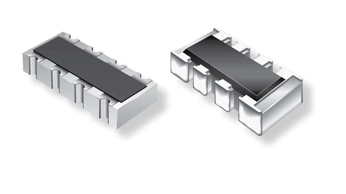
Resistor networks and resistor arrays combine two or more resistive elements in one component package. They reduce component count, placement operations and PCB area, while short internal connections can simplify routing and improve element-to-element thermal coupling.
A resistor array usually contains several nominally independent resistors, either isolated or connected to one common terminal. A resistor network may implement a defined internal circuit, such as a voltage divider, dual terminator, R-2R ladder, attenuator or matched feedback network. This distinction is important: a low-cost pull-up array and a precision divider network may look similar externally, but their electrical specifications and intended applications are very different.
Most new high-density designs use SMD chip resistor arrays. Through-hole SIL/SIP and DIL/DIP networks remain relevant for legacy equipment, socketed boards and selected industrial applications. Thick-film technology dominates cost-sensitive general-purpose arrays, whereas thin-film and metal-foil networks are used where ratio accuracy, low ratio drift, low noise or long-term stability are critical. For a broader introduction to film technologies, see thin-film, thick-film and metal-foil resistor technologies.
Key Takeaways
- Resistor networks and resistor arrays combine multiple resistive elements into one package, saving PCB area and reducing component count.
- A resistor array includes isolated or bussed resistors, while a resistor network has defined internal circuits for specific applications.
- High-density designs prefer SMD chip resistor arrays, while through-hole options are used for legacy applications.
- Choosing between thick film, thin film, and metal foil technologies depends on cost, precision, and application requirements.
- Key specifications for selecting a resistor network include internal topology, resistance values, and tolerance, impacting application performance.
By a network we mean several separate or mutually connected resistor elements collected in a common casing and supplied with terminal leads to each element. Usually the elements have the same resistance value but different values may exist, for example a number of R1 and R2 connected in a ladder pattern that gives a certain voltage division.
In hybrid manufacturing the customer himself applies the resistor elements in a desired casing.
Resistor Array vs. Resistor Network
The terms resistor array and resistor network are often used interchangeably in catalogues, but separating them helps designers select the right component class.
| Term | Typical internal arrangement | Main reason to use it | Typical examples |
|---|---|---|---|
| Isolated resistor array | Several electrically independent resistors in one package | PCB density, reduced placement count and simplified procurement | LED current limiting, GPIO pull-downs, bias resistors |
| Bussed resistor array | Several resistors connected to one shared terminal | Common pull-up or pull-down rail with compact routing | Microcontroller inputs, open-drain signals, address or control lines |
| Dual terminator network | Two or more resistors connected to a defined common node | Line biasing or termination where the specified topology is required | Legacy bus interfaces and selected communications circuits |
| Matched divider network | Two or more ratioed resistors on a common substrate | Accurate division ratio and low temperature-induced ratio drift | ADC scaling, voltage references, battery sensing |
| Precision feedback network | Matched resistors with specified ratio tolerance and tracking | Stable gain, CMRR and filter response | Instrumentation amplifiers, differential amplifiers, active filters |
| R-2R ladder network | Repeated R and 2R values in a controlled ratio | DAC linearity and monotonicity | Precision DACs and programmable analogue circuits |
Design note: A common terminal does not automatically make an array suitable for signal termination. Check the exact internal schematic, resistance values, voltage ratings, parasitic parameters and the relevant interface standard before selecting a bussed part.
General comments
Resistor networks are manufactured both for hole mount and as SMDs. Most parts are manufactured in thick film but thin film as well as metal foil types have a good market.
Discrete SM components may be mounted in the network package. But usually the planar substrates are screen printed with a network pattern either with a metal powder paste that is fired to metal glaze/thick film. Or metal foils are glued to the planar substrate or metal films of NiCr or Ta2N are vaporized or ion implanted – sputtered – on the substrates. Thick-film resistor arrays are normally made by screen-printing a resistive paste onto a ceramic substrate and firing it to form the resistive film. Precision values may be obtained by laser trimming, although the degree of trimming depends on the product family and required specification. Thin-film networks use a deposited metallic resistive layer, commonly a nickel-chromium alloy, patterned by photolithography or etching. Metal-foil networks use a precision foil pattern bonded to a stable substrate and are intended for the most demanding ratio, drift and noise requirements.
Each technology involves trade-offs. Thick film is widely used for general-purpose arrays because it is economical and robust. Thin film is preferred where lower noise, tighter tolerance and improved stability are required. Metal foil addresses high-end precision applications where ratio stability and very low drift justify higher cost.
Technology Selection
| Technology | Strengths | Limitations | Typical network applications |
|---|---|---|---|
| Thick film | Cost-effective, broad resistance range, widely available, generally robust for routine biasing and logic functions | Higher noise and greater drift or non-linearity than precision thin-film or foil technologies | Pull-up/pull-down arrays, LED biasing, general-purpose control and consumer electronics |
| Thin film | Tighter tolerance, lower noise, improved stability and lower TCR options | Usually higher cost and may require more conservative pulse and power derating | Feedback networks, precision dividers, ADC/DAC interfaces and instrumentation |
| Metal foil | Excellent ratio stability, very low drift and low excess noise | Higher cost, fewer package and value options | Metrology, precision measurement, high-end analogue and reference circuits |
For technology trade-offs involving tolerance, TCR, noise, linearity, pulse capability and long-term drift, see the resistor technology selection and benchmark guide.
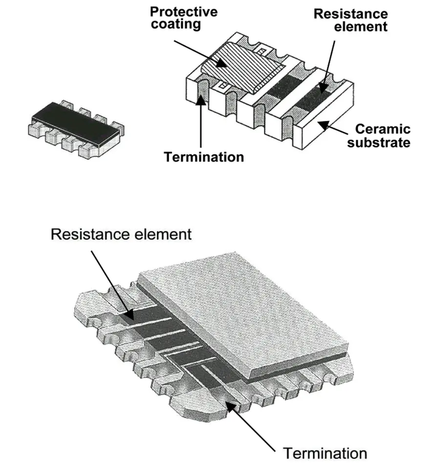
Just as the chips the resistor element films are protected by a glass coat or sometimes a tantalum oxide coating.
Package Families
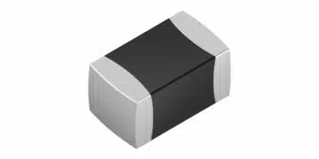
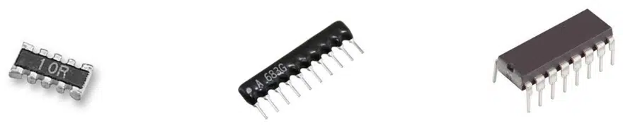
SMD chip resistor arrays are the preferred option for most new compact electronics. They combine two, four, eight or more resistor elements in a small surface-mount body and can reduce placement count substantially compared with individual chip resistors. Common arrangements include isolated elements and bussed elements with one common terminal.
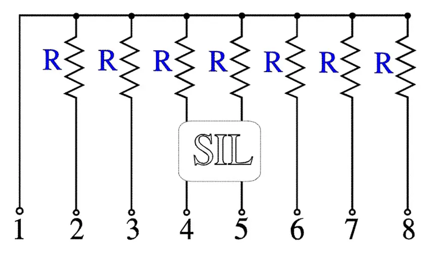
SIP or SIL networks place terminals in a single row. They are useful where through-hole assembly, manual servicing or legacy footprints are required, but their height and leaded construction make them less attractive for modern dense surface-mount assemblies.
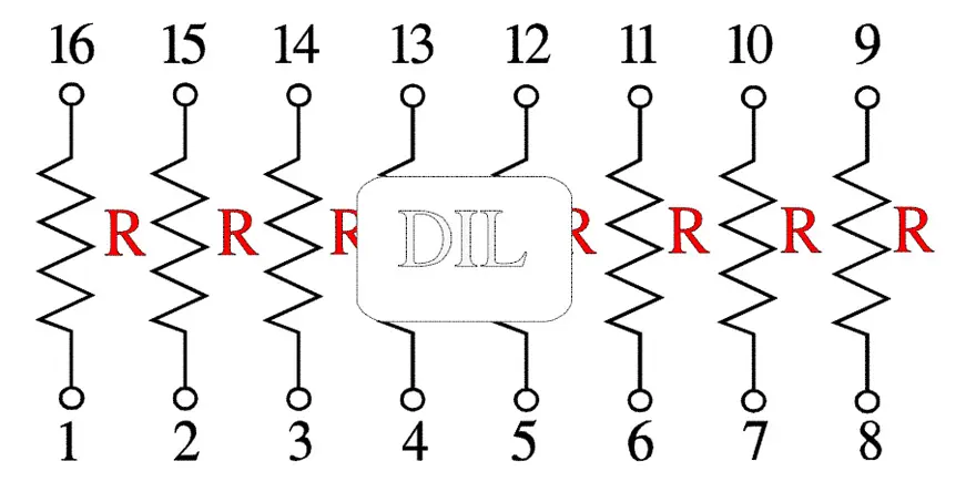
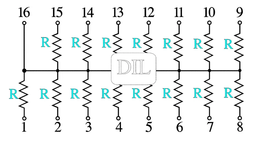
DIP or DIL networks use two parallel rows of leads and are mainly encountered in legacy digital boards, industrial equipment and selected socketed applications. They can offer many elements in one package but occupy significantly more PCB area than SMD arrays.
Precision hybrid and hermetic networks may use ceramic substrates, moulded packages or hermetic housings. These products are selected for controlled ratio accuracy, low tracking error, high reliability or demanding environmental requirements rather than for lowest cost.
PCB material note: Standard SMD resistor arrays are routinely mounted on FR-4 PCBs. Ceramic substrates may be appropriate in specialised high-temperature, RF, power-dense or coefficient-of-thermal-expansion-sensitive designs, but they are not a general requirement for SMD resistor networks. The more important considerations are PCB flex, land pattern, solder-joint geometry, local thermal gradients and the manufacturer’s assembly guidance.
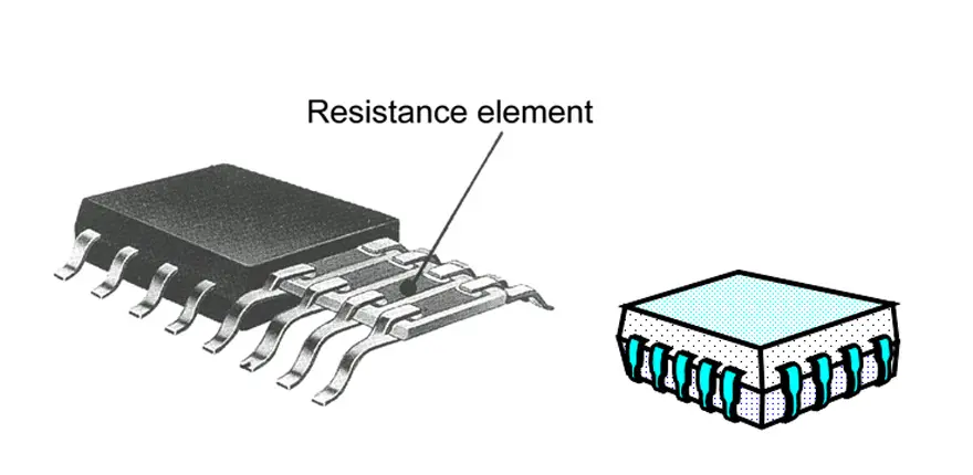
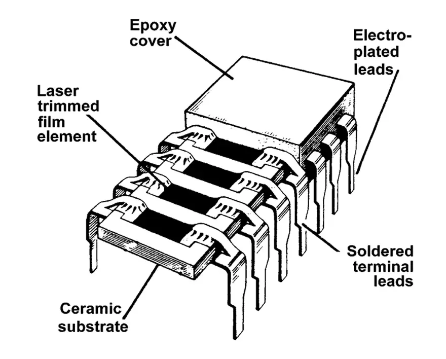
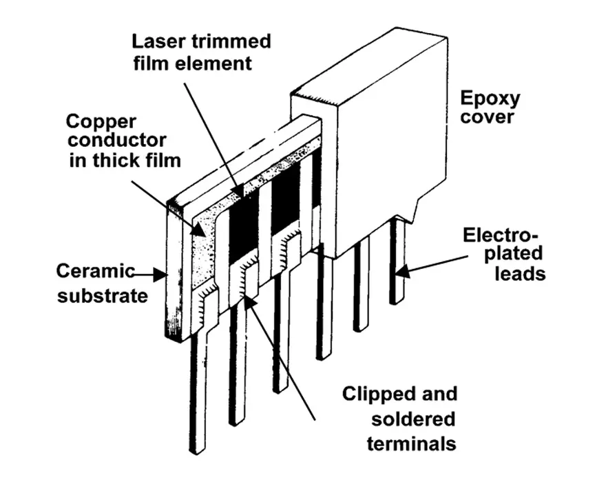
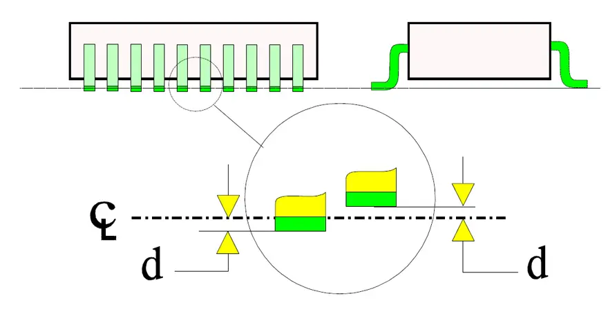
Of all requirements that have to be specified and checked there is one that is of particular interest: The coplanarity , i.e., the mutual planarity of the leads relatively to a reference plane. If this measure is not met – d in Figure 6. – some leads will be suspended in the air at soldering to the substrate. The measure is exemplified by the gull-wing shape but applies as well to the J hook design.
Configurations
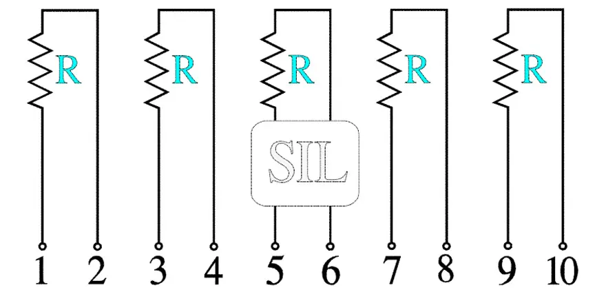
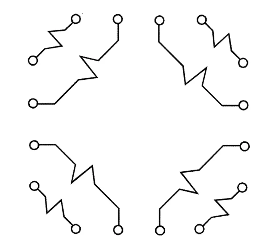
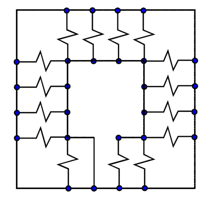
The electrical circuit can be arranged in an infinite number of ways. Usually the resistor values are mutually equal. Sometimes they are bussed (common neutral), sometimes they are arranged separately. Figures 7. to 12. show examples of the most common configurations.
Characteristics
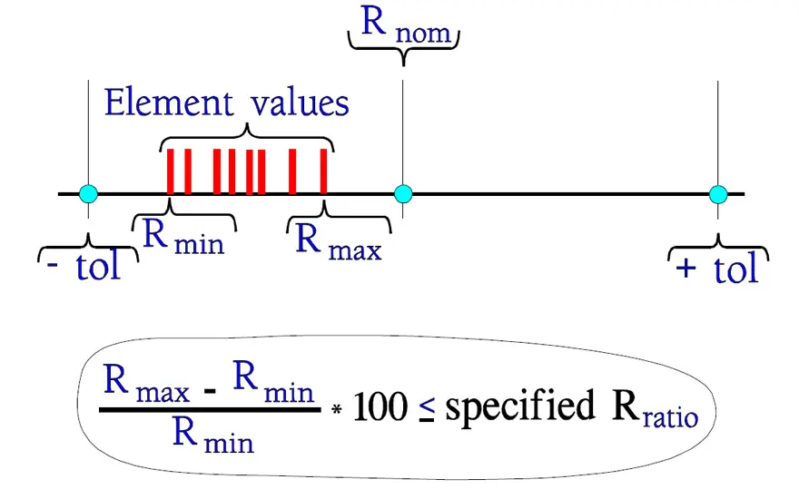
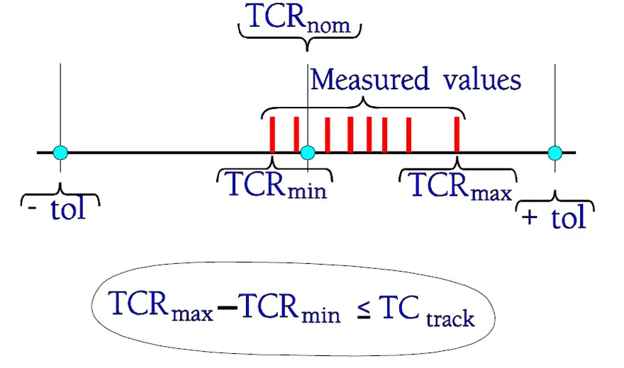
In the first place the characteristics of the networks are determined by the resistor material that rules the TCR and the absolute tolerance. Because the elements included belong to the same manufacturing batch their parameter distribution is much more limited than that of the total production. This enables an additional kind of specification that often is used with precision components: the resistance ratio or relative tolerance and the TCR tracking. The concepts are illustrated in Figures 13. and 14.
In order to understand the resistance ratio concept better we should recollect how the absolute tolerance is constructed. If the actual resistance is called R and the nominal resistance Rnom, the ratio R/Rnom should be within the tolerance limits. With the relative tolerance, however, we mean a comparison of the different element resistances, Rr, with a reference element, Rref, in the network. Rref usually is the first element in the schematic.
The ratio Rr/Rref is called the resistance ratio accuracy, ratio tolerance (or relative tolerance) and is expressed in percent. It is a comparison of magnitude and therefore is given without a sign. If the element values of the network are distributed as in Figure 19. we realize that the largest spread will occur if Rref = Rmin and Rr = Rmax. Thus the resistance ratio accuracy, Rratio, shall fulfill the condition (Rmax – Rmin)/Rmin ≤ Rratio.
Specifications That Matter
A resistor network datasheet must be read at two levels: the specifications of each individual element and the limits that apply to the complete package. The required priority depends on whether the network is used for simple logic biasing, precision analogue scaling, power dissipation or high-speed signalling.
| Parameter | What it describes | Why it matters |
|---|---|---|
| Resistance value and tolerance | Nominal resistance and allowable absolute deviation of an element | Sets bias current, divider current, time constant and initial circuit accuracy |
| Ratio tolerance | Initial accuracy of one element relative to another element in the same network | Often dominates divider, gain, R-2R ladder and differential-amplifier accuracy |
| Absolute TCR | Resistance change of an individual element over temperature | Important when an absolute resistance value controls current, timing or a reference level |
| TCR tracking or ratio drift | Difference in temperature behaviour between elements | Critical when circuit performance depends on a resistance ratio rather than an absolute value |
| Power per element | Allowed continuous dissipation in one resistor | Prevents local overheating and resistance drift |
| Total package power | Maximum permitted dissipation of all active elements together | Limits multi-channel use; it is not necessarily the sum of individual ratings |
| Working and overload voltage | Maximum steady-state and short-duration voltage limits | Essential in dividers, sensing circuits and fault conditions |
| Pulse and surge capability | Permitted energy or pulse waveform under defined test conditions | Important near relays, inductive loads, power rails and exposed I/O |
| Long-term drift | Change in resistance after load-life, humidity or temperature testing | Determines whether initial accuracy remains adequate over product life |
| Parasitic inductance and capacitance | Non-ideal electrical behaviour at high frequency | Can affect termination, RF attenuation, edge rate and channel-to-channel coupling |
Important: Do not select a precision network from absolute tolerance alone. For a divider, differential amplifier or R-2R DAC, compare ratio tolerance and specified TCR tracking over the complete operating-temperature range. Treat broad technology ranges only as orientation; use the actual manufacturer datasheet for the selected series and resistance values.
For a refresher on how resistance can vary with applied voltage and frequency, see resistor voltage and frequency dependence.
Table 1 summarises the specifications and design checks that most often determine whether a resistor array or resistor network is suitable for a given application. The selected component datasheet remains the controlling source for ratings, test conditions and derating rules.
| Selection criterion | What to check in the datasheet | Most important for | Common design mistake |
|---|---|---|---|
| Internal topology | Isolated, bussed, divider, dual terminator, R-2R ladder, attenuator or another defined circuit; verify pinout and common-terminal location. | All applications; especially pull-up arrays, termination networks and precision analogue circuits. | Assuming that components with similar packages have the same internal connection. |
| Number of elements | Number of resistor elements, number of terminals and whether all elements can be used independently. | GPIO biasing, LED current limiting, multi-channel signal conditioning and dense control boards. | Selecting an eight-element package when the required circuit topology only supports fewer usable channels. |
| Resistance value | Nominal value, available E-series values and whether all elements have equal values or a defined ratio. | Pull-ups, pull-downs, LED biasing, timing, voltage dividers and R-2R networks. | Using a common-value array where unequal values or a controlled ratio are required. |
| Absolute tolerance | Permitted deviation of each individual resistor from its nominal resistance value. | Bias current, timing, current limiting and circuits dependent on absolute resistance. | Using absolute tolerance as the only accuracy criterion in a ratio-dependent circuit. |
| Ratio tolerance | Initial accuracy of the resistance ratio between specified elements in the same network. | Voltage dividers, differential amplifiers, gain-setting networks and R-2R DACs. | Assuming two individually accurate resistors automatically provide an accurate ratio. |
| Absolute TCR | Temperature coefficient of each resistor element, normally specified in ppm/°C over a stated temperature range. | Current-setting, timing and reference circuits where the absolute resistance must remain stable. | Comparing TCR values without checking the stated temperature range and resistance value. |
| TCR tracking / ratio drift | Difference in temperature behaviour between resistor elements; check the maximum value and specified temperature range. | Precision dividers, instrumentation amplifiers, bridge circuits, ADC scaling and DAC ladders. | Using absolute TCR as a substitute for tracking specification. |
| Power per element | Maximum continuous dissipation permitted in one active resistor element, including temperature derating. | LED current limiting, bias networks, analogue scaling and multi-channel loads. | Checking only total package |
Selection rule: For simple pull-up, pull-down and low-power bias functions, topology, resistance value, voltage rating and package dissipation are usually decisive. For precision dividers, gain networks and R-2R ladders, prioritise ratio tolerance, TCR tracking, self-heating behaviour and long-term ratio stability.
Ratio Accuracy, Tracking and Self-Heating
Precision networks are valuable because their resistor elements are fabricated on a common substrate and experience similar environmental conditions. However, common construction does not eliminate all ratio error in the finished circuit. The most important residual error mechanism is unequal self-heating.
For a first-order estimate, temperature-induced ratio error can be expressed as:
If one resistor in a divider or feedback network dissipates much more power than its partner, the two elements can operate at different temperatures. This creates an additional ratio shift even if the datasheet specifies excellent TCR tracking under uniform ambient conditions.
- Distribute dissipation as symmetrically as practical when ratio accuracy is important.
- Keep precision networks away from hot MOSFETs, inductors, power resistors and forced-air thermal gradients.
- Use a network with suitable package power margin; high local temperature can increase drift even when the nominal rating is not exceeded.
- Keep high-impedance divider nodes clean and short to reduce leakage from contamination, flux residue and board surface moisture.
- Use Kelvin connections where PCB trace resistance could become part of a precision sensing or feedback ratio.
Applications of Resistor Networks
Digital Pull-Up and Pull-Down Arrays
Microcontrollers, FPGAs, logic devices and bus transceivers often require multiple pull-up or pull-down resistors. A bussed resistor array can connect several signal lines to one common supply or ground terminal, reducing routing congestion and placement count. The key requirements are resistance value, voltage rating, logic leakage budget, package power and the correct common-terminal polarity.
LED Biasing and General-Purpose Signal Conditioning
Isolated arrays can replace several discrete resistors in low-power LED, transistor-base, analogue-bias and signal-conditioning circuits. They are most attractive when channel currents are modest and all elements use similar values. Verify both the dissipation of each active element and the allowed dissipation of the entire package.
ADC Scaling and Reference Dividers
Matched divider networks are useful when an ADC input, voltage reference or battery-monitoring circuit depends on a stable resistance ratio. Ratio tolerance sets the initial scale-factor error, while TCR tracking controls the ratio change with ambient temperature. In high-voltage dividers, also check the permitted working voltage per element, overload capability, creepage and clearance, and the effect of leakage across the PCB surface.
Op-Amp Gain and Differential Amplifiers
In differential amplifiers, instrumentation amplifiers and active filters, resistor ratios set gain, common-mode rejection and frequency response. A matched thin-film or foil network can maintain these relationships more consistently than unrelated discrete resistors. This is especially relevant where small ratio mismatch can limit CMRR or introduce gain drift over temperature.
DAC R-2R Ladders
R-2R networks require accurate and stable relationships between R and 2R values. Ratio error and ratio drift can directly affect linearity, monotonicity and differential non-linearity. Select a purpose-designed precision network where the converter accuracy cannot tolerate the accumulated mismatch of discrete resistors.
Communication Bias and Termination
Resistor networks can implement bias or termination functions in selected communication circuits, but the topology must match the relevant interface specification. A compact package may shorten routing, yet internal capacitance, shared terminals and channel coupling can be undesirable at high edge rates. For differential interfaces, use the correct differential termination arrangement rather than assuming a general bussed array is suitable.
Automotive and Industrial Electronics
Automotive ECUs, industrial controllers and sensor modules use resistor arrays for input biasing, microcontroller pull-ups, status indication and analogue scaling. In harsh environments, verify temperature range, moisture and sulfur robustness, load-life drift, vibration performance and any required AEC-Q200 qualification. The resistor selection guide for qualification, pulse and reliability requirements provides a useful broader framework.
Assembly and Reliability Considerations
Resistor networks reduce the number of mounted components, but their multi-element construction makes correct assembly, derating and PCB layout important. Failure analysis should distinguish between resistance drift, solder-joint defects, ceramic cracking and circuit-level ratio error.
| Failure mechanism | Typical causes | Possible symptom | Prevention |
|---|---|---|---|
| Resistance drift | Continuous overload, repeated pulses, high operating temperature, humidity or contamination | Gain error, bias shift, calibration loss or incorrect threshold | Derate power and voltage, check load-life data, choose technology appropriate to the environment |
| Open circuit or intermittent contact | PCB flex, thermal cycling, cracked ceramic body, damaged termination or solder-joint fatigue | Temperature-dependent intermittent failure, missing pull-up or unstable signal | Keep arrays away from board edges, mounting holes, connectors and depanelisation stress; follow recommended land patterns |
| Solder-joint defect | Incorrect reflow profile, insufficient or excessive solder paste, pad imbalance or poor coplanarity in leaded packages | High or unstable contact resistance, open circuit or early thermal-cycle failure | Use supplier reflow guidance and recommended footprint; validate assembly using normal production inspection methods |
| Ratio shift in a precision circuit | Unequal element self-heating, local thermal gradient, leakage, contamination or excessive voltage coefficient | Gain drift, reduced CMRR, ADC scale-factor shift or DAC non-linearity | Use matched networks, arrange power symmetrically, keep nodes clean and assess worst-case temperature conditions |
| Pulse or surge damage | Inductive switching, relay contacts, ESD-related events, fault transients or inrush conditions | Permanent resistance shift, open circuit or short circuit | Check waveform-specific pulse ratings; add appropriate circuit protection rather than relying on a general-purpose array |
PCB flex is a particularly important issue for ceramic-based SMD components. Avoid placing resistor arrays close to board edges, mounting screws, connectors, scored depanelisation lines and areas subject to manual flexing. For automotive or other severe environments, review the relevant qualification tests and the component manufacturer’s board-flex guidance.
Do not treat conformal coating or encapsulation as a universal corrective action. It may improve environmental protection in a qualified design, but it can also add mechanical stress, complicate inspection and affect rework.
Conclusion
Resistor arrays provide an efficient way to integrate multiple general-purpose resistors in a compact PCB area, while precision resistor networks provide controlled resistance ratios and temperature tracking for analogue, measurement and data-conversion circuits.
Start selection with the required internal topology, then verify resistance values, ratio tolerance, TCR tracking, working voltage, element power, total package dissipation, pulse capability, thermal environment and assembly constraints. A component that is suitable for simple pull-up functions may be unsuitable for precision gain setting, high-voltage scaling or high-speed termination.
Always use the selected manufacturer datasheet as the governing source for pinout, ratings, derating curves, test conditions and recommended PCB footprint.
Further Reading
- SMD Chip Resistors: Construction, Ratings and Selection Considerations — explains package construction, resistance values, tolerance, TCR, power rating and SMD assembly issues.
- Thin-Film, Thick-Film and Metal-Foil Resistor Technologies — compares the primary resistor-film technologies used in arrays and precision networks.
- Resistor Technology Selection and Benchmark Guidelines — helps compare thick film, thin film and foil resistors by precision, stability, pulse performance and reliability requirements.
- Carbon, Metal Oxide and Other Resistor Technologies — provides additional context for high-resistance, high-voltage and specialised resistor applications.
- How Qualification Supports Reliable Thick-Film Resistor Selection — discusses qualification, reliability and environmental performance relevant to demanding resistor-array applications.
References
- Thin Film and Metal Film Resistors, Passive Components Blog.
- SMD Chip Resistors, Passive Components Blog.
- Resistor Technology Selection and Benchmark Guidelines, Passive Components Blog.
- Carbon, Metal Element, Metal Oxide, Metal Foil Resistors, Passive Components Blog.
- Selection of Thick-Film Resistors Based on Qualification, Passive Components Blog.
- Networks and Arrays — Thick Film, Vishay Intertechnology.
- Networks and Arrays — Thin Film, Vishay Intertechnology.
- Resistor Networks, Bourns.
- Resistor Networks, Panasonic Industry.
Technical ratings, availability and qualification status vary by product series, package, resistance value and manufacturer revision. Consult the current datasheet for the selected component before final design release.
FAQ About Resistor Networks
A resistor array usually contains several independent or bussed resistors in one package, primarily to save PCB area and placement operations. A resistor network may contain a defined internal circuit such as a divider, dual terminator, R-2R ladder or matched feedback arrangement, where ratio accuracy and temperature tracking are important.
Use a bussed array when several signal lines require the same pull-up or pull-down resistor connected to one common supply or ground terminal. Confirm the common-terminal pin, the required logic voltage, leakage current, resistance value and total package dissipation.
Ratio tolerance is the initial accuracy of the resistance relationship between two elements in a network. It is especially important in voltage dividers, differential amplifiers, instrumentation amplifiers and R-2R DAC ladders, where circuit performance depends more on the resistor ratio than on the absolute value of either resistor.
Absolute TCR describes how much the resistance of one element changes with temperature. TCR tracking describes how closely the temperature behaviour of two or more elements matches. A precision divider can have a moderate absolute TCR yet still maintain a stable division ratio if its elements have very close tracking.
Not automatically. Each element must remain within its individual continuous-power rating, and the combined dissipation must remain below the manufacturer’s total package-power rating after applying the specified temperature derating. The permitted package dissipation may be lower than the arithmetic sum of all individual element ratings.
Check the voltage across every individual resistor element, not only the total supply voltage. Confirm the maximum working voltage, overload voltage, maximum element-to-element voltage where specified, and the power dissipated in each element. High-voltage dividers also require adequate PCB creepage, clearance and control of surface leakage.
When network elements dissipate unequal power, they can operate at different temperatures. This temperature gradient can change the resistance ratio and introduce gain or scale-factor error even when the network has good specified TCR tracking. Use adequate power margin and distribute dissipation as symmetrically as practical.
They can reduce external routing length and component count, but their internal geometry also introduces parasitic capacitance, inductance and possible coupling between channels. For high-speed, RF or precision-termination functions, check frequency-related data, package geometry and PCB layout rather than relying on the array format alone.
No. Standard SMD resistor arrays are commonly mounted on FR-4 PCBs. Ceramic substrates can be appropriate for specialised high-temperature, RF or power-dense assemblies, but the normal priorities are correct footprint design, controlled soldering, avoidance of board flex and management of thermal gradients.
Avoid mechanically stressed areas near board edges, mounting holes, connectors, scored depanelisation lines and locations subject to repeated manual flexing. For precision networks, also avoid local heat sources such as power MOSFETs, inductors and high-power resistors, unless thermal symmetry has been evaluated.
Thin-film networks are widely used when tight tolerance, low noise and good ratio stability are required. Metal-foil networks are selected for the most demanding low-drift and low-noise applications. Thick-film arrays remain the economical default for general-purpose biasing, pull-up and pull-down functions.
How to Select and Implement Resistor Networks
- Define the circuit function.
Decide whether the requirement is simply multiple resistors in less area, a common pull-up or pull-down function, a matched divider, a precision feedback ratio, an R-2R ladder, or a specific termination topology.
- Verify the internal topology and pinout
Select isolated, bussed, divider, dual-terminator or ratioed elements as required. Verify the internal schematic, common-terminal position and pinout in the manufacturer datasheet before designing the PCB footprint.
- Set the accuracy budget.
For routine biasing, absolute resistance tolerance and TCR may be sufficient. For dividers, differential amplifiers, ADC scaling and DAC ladders, define the permitted ratio tolerance, TCR tracking, long-term drift, voltage coefficient and self-heating error.
- Check power, voltage and pulse stress.
Calculate voltage and continuous power in every active resistor element. Confirm per-element power, total package dissipation, temperature derating, working voltage, overload voltage and any waveform-specific pulse or surge rating.
- Select the resistor technology.
Use thick film for cost-sensitive general-purpose functions, thin film for improved precision and lower noise, and metal foil where exceptional ratio stability and low drift are necessary. Select only a technology whose published ratings meet the required operating conditions.
- Assess layout and high-frequency effects.
For high-speed or sensitive analogue circuits, assess package capacitance, inductance, channel coupling, shared-terminal effects, trace symmetry and return-current paths. A compact network does not automatically guarantee better signal integrity.
- Design for assembly reliability.
Use the recommended PCB footprint and soldering profile. Keep ceramic resistor arrays away from board edges, mounting points, connectors, depanelisation lines and other areas exposed to PCB flex or severe thermal gradients.
- Validate on the final PCB.
Measure the required resistance ratio, gain, divider accuracy or signal performance across the intended temperature range and operating power. For demanding products, include appropriate load-life, humidity, vibration, thermal-cycle and pulse testing.