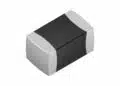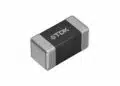





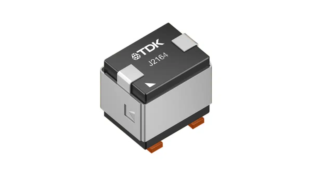
TDK’s new EP21 series SMD common‑mode chokes targets high‑current low‑voltage EMI filtering where PCB area and thermal performance are critical.
The flat‑wire double choke construction, underbody termination and four‑pin SMD design make these parts attractive for modern DC‑DC converters and compact EMC protection circuits according to the manufacturer press release.
Key features and benefits
- High current handling up to 35 A at low DC resistance, supporting high‑power DC‑DC stages without excessive conduction loss.
- Low DC resistance down to 0.44 mΩ, helping reduce copper loss and ease thermal design in dense layouts.
- Wide inductance range from 160 µH to 640 µH, allowing engineers to trade off impedance profile and current rating for different converter topologies.
- Flat‑wire winding on MnZn ferrite core, improving fill factor and thermal paths compared to classic round‑wire coils, with MnZn ferrite optimized for common‑mode suppression in the 100 kHz–MHz range.
- SMD format with underbody termination, reducing footprint to 23.8 x 17.7 mm and simplifying automated assembly versus through‑hole chokes.
- Four‑pin design for mechanical robustness, providing stable solder joints and good coplanarity on the PCB, important for high‑mass magnetics in reflow processes.
- Impedance peak in the 500 kHz–3 MHz region, matching typical switching frequency bands and harmonics of modern DC‑DC converters and low‑voltage power electronics.
Typical applications
The EP21 common mode choke series is aimed at common‑mode noise suppression in low‑voltage high‑current systems. Typical use cases include:
- Common‑mode input or output filters in non‑isolated DC‑DC converters (step‑down/step‑up regulators).
- EMC protection in low‑voltage power distribution rails in industrial and telecom equipment.
- Common‑mode filtering on battery and DC bus connections in e‑mobility or robotics, where currents above 20 A are common.
- Noise suppression on auxiliary low‑voltage supplies in larger power systems with fast power stages.
- Compact common‑mode filtering in rack‑mount or module‑based PSU designs that need SMD assembly for high throughput.
In practice, these chokes sit in series with both lines of a differential pair (for example, +V and return) and primarily attenuate common‑mode components while keeping differential‑mode impedance relatively low.
Technical highlights
Electrical ratings
- Rated voltage: 48 V AC and 80 V DC, suitable for typical low‑voltage DC buses (48 V telecom, 48 V industrial systems, higher‑current 24 V rails with transient margins).
- Rated current: 20.3 A to 35.0 A across the series, without derating up to +70 °C according to the manufacturer datasheet.
- Temperature behavior: No derating required up to +70 °C; above this point derating must be applied, which is important when placing the component near hot power devices.
- DC resistance (typical): 0.44 mΩ to 1.75 mΩ across types, directly influencing I²R loss and temperature rise.
- Rated inductance: 160 µH to 640 µH per common‑mode winding, with average stray inductance down to 200 nH.
- Stray inductance (average): 200 nH to 900 nH, indicating relatively low differential‑mode inductance so the choke primarily acts on common‑mode noise.
- Impedance peak frequency: Maximum impedance occurs between 500 kHz and 3 MHz depending on type, aligning with typical switching frequencies and their harmonics.
Mechanical and construction data
- Package format: SMD double choke with four pins.
- Footprint: 23.8 x 17.7 mm for all variants.
- Height: Between 21.6 mm and 22.3 mm, enabling relatively compact vertical integration compared with classic bobbin chokes.
- Underbody termination: Terminals located under the component body, minimizing lateral pad area and allowing dense placement.
- Core material: MnZn ferrite, a standard choice for power/common‑mode inductors balancing permeability and loss at targeted frequency ranges.
- Winding technology: Flat‑wire, improving current density, lowering AC resistance and supporting better thermal paths than equivalent round‑wire designs.
EP21 series overview table
| Ordering code | Rated current [A] | Inductance [µH] | DC resistance [mΩ] | Stray inductance (AVG) [nH] | Dimensions L x W x H [mm] |
|---|---|---|---|---|---|
| B82552J2164J021 | 35.0 | 160 | 0.44 | 200 | 23.8 x 17.7 x 22.3 |
| B82552J2284J021 | 30.8 | 280 | 0.80 | 390 | 23.8 x 17.7 x 21.9 |
| B82552J2444J021 | 23.5 | 440 | 1.25 | 500 | 23.8 x 17.7 x 21.7 |
| B82552J2644J021 | 20.3 | 640 | 1.75 | 900 | 23.8 x 17.7 x 21.6 |
This table illustrates the trade‑off between current rating, inductance and DC resistance: higher inductance variants provide more common‑mode impedance at lower frequencies at the expense of higher DC resistance and lower rated current.
Variant selection table (design perspective)
| Design priority | Recommended variants | Comment |
|---|---|---|
| Maximum current, minimal loss | B82552J2164J021 | Best suited for highest load currents and hot spots |
| Balanced current vs inductance | B82552J2284J021, B82552J2444J021 | Good middle ground for typical DC‑DC converter rails |
| Highest common‑mode impedance | B82552J2644J021 | For strongest suppression where current margin is available |
This table is a qualitative indication based on the electrical data; final choice should be confirmed against the specific EMC and thermal requirements of the target design.
Design‑in notes for engineers
- Define noise profile first: Measure or simulate common‑mode noise spectra of the DC‑DC converter or power rail. Choose the EP21 variant whose impedance peak aligns with the dominant noise frequencies, keeping in mind that these parts peak between 500 kHz and 3 MHz.
- Check current and temperature margins: Use the rated current and DC resistance values to estimate conduction losses P=I2⋅R and temperature rise at full load. Ensure operation within the no‑derating region up to +70 °C or apply appropriate derating curves from the manufacturer datasheet for higher ambient temperatures.
- Place carefully in the layout: Given the height and mass of the EP21 components, ensure solid pad design, sufficient solder fillet and mechanical support, especially in applications subject to vibration or shock.
- Consider stray inductance impact: While stray inductance is relatively low, it can still introduce differential‑mode impedance at high frequencies. In fast‑edge digital or very low‑voltage rails, verify that voltage drops and ringing remain acceptable.
- Combine with differential‑mode elements where needed: Common‑mode chokes often work together with X/Y capacitors or dedicated differential‑mode inductors. The EP21 series provides the common‑mode element; overall EMC performance depends on the complete filter design.
- Account for underbody termination during PCB design: Ensure correct land pattern as specified in the datasheet so that the underbody contacts wet properly and solder inspection is feasible. Pay attention to solder mask definition and stencil thickness.
- Verify creepage and clearance: While these components are intended for low‑voltage applications, it is still essential to check creepage/clearance distances and insulation specifications according to the applicable standards for the end equipment.
- Use manufacturer tools and data: TDK’s design tools and product catalog entries can help refine the choice of part number, especially when optimizing for EMC compliance in complex systems.
Source
This article is based on the official TDK Electronics press release and associated product information for the EP21 series SMD common‑mode chokes, with additional independent editorial context for design engineers and purchasers.