


This article elaborates on design and calculation of buck DC/DC converters. The post is based on Würth Elektronik‘s “DC/DC Converter Handbook” that can be ordered from WE website here. Published under permission from Würth Elektronik.
Key Takeaways
- The article discusses Buck Converter Design based on Würth Elektronik’s DC/DC Converter Handbook.
- It emphasizes minimizing high ΔI/Δt loops and the hot node area for better EMC performance and efficiency.
- Proper selection of input/output capacitors and inductors is crucial for ripple control and EMC compliance.
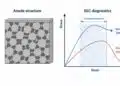
- Inductor selection requires defining six operating parameters and verifying inductance, saturation current and RMS current against datasheet curves for both DC bias and temperature rise.
- A 5-step practical inductor selection procedure is provided, illustrated with an automotive 5 V / 4 A example using a TT Electronics AEC-Q200 qualified part.
- Simulation tools like REDEXPERT help simplify and validate component selection.
- Designing input and output filters is essential to meet EMI/EMC standards while maintaining converter efficiency.
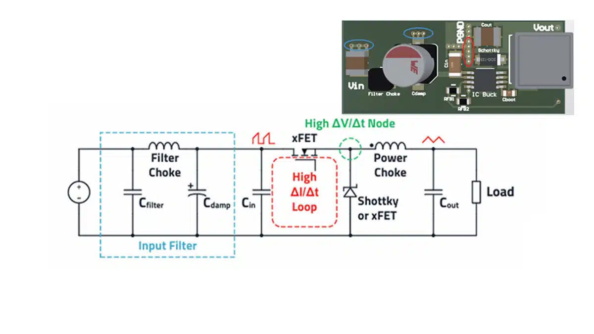
Buck Converter Block Diagram and General Thoughts
Among the switched-mode power supplies (see DC-DC Converter Basic Characteristics and Formulas), the buck converter (step-down converter) is certainly the most widely used topology. The buck converter is basically nothing more than a square wave generator with a downstream LC filter.
It is obvious at first glance that, with regard to EMC, more attention must be paid to the input side than to the output side. From a functional perspective, “only” one capacitor is required at the input. This capacitor buffers the charge necessary for the current during the switch-on phase of the high-side FET and is recharged by the source during the switch-off phase.
If this converter is now placed at the input of the entire device electronics (e.g., Vin = 24 V) then further precautions must be taken regarding interference emission (EN 55032) and interference immunity (EN 55035). Even a suitably selected and well placed input capacitor is not sufficient to buffer the sometimes very high discontinuous currents over a wide frequency range.
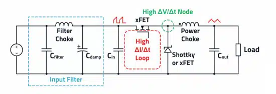
As apparent in figure 3., a current loop (H-field loop antenna) with a very high ΔI/Δt results at the input of the buck converter.
Thus, even the smallest parasitic inductance of the input capacitor (ESL) and circuit board layout can lead to unwanted RF voltages up to over 200 MHz. This is one major cause of differential mode interference. For this reason, a compact layout, the appropriately selected capacitor technology (aluminum polymer capacitors or MLCC ceramic capacitors) as well as a correctly designed input filter are essential for success. The compact layout also minimizes the radiated field via the undesirable conductor loop (H-field loop antenna).
A filter may also be required at the output of the buck converter if, for example, the residual ripple of the output voltage must be particularly low.
There is the “hot node” – marked green in the block diagram – at the connection of the source terminal of the internal or external high-side MOSFET and the cathode terminal of the diode, or in case of a synchronous buck, the drain terminal of the second MOSFET. The switched input voltage can be measured in full amplitude at this point. The switching voltage has a particularly high ΔV/Δt here, creating an undesirable E-field antenna.
The conductor traces and copper surfaces of the PCB together with the PCB material used (e.g., FR4) give rise to undesirable parasitic capacitances. An RF current flows to the reference ground via these coupling capacitances. This current is the main cause of common-mode interference, which appears in EMC measurements. Therefore, it is important to minimize the area of this point in the layout.
The “dot” mark on the storage inductor is the start of the (inside) winding and should be aligned or connected toward the “hot node”. This helps to keep the geometric area of this critical structure around the “hot node” and thus the parasitic capacitance, as well as the resulting E-field antenna structure, as small as possible.
Buck Converter Layout Considerations
In the layout of a buck converter, it is therefore important to keep the loops with a high ΔI/Δt, as well as the geometric area of the “hot node” with its high ΔV/Δt, as small as possible.
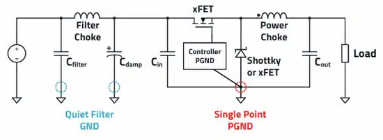
As apparent in Figure 1.30, the “single point“ ground reference for the power ground is the way to success. If the configuration of the input capacitor, the output capacitor, the diode, and the IC are placed skillfully, the ground pads of these components meet at just one point. This minimizes undesirable H-field loops as well as parasitic inductances as much as possible.
If an input filter is used, it should be placed some distance away from the buck. As a result, the ground reference of the filter capacitors stays largely quiet and the risk of direct field coupling into the filter components is reduced. The individual filter components (in this case, filter inductor and filter capacitor) should always be configured at 90° to each other; this avoids unfavorable coupling and provides a wideband filter effect.
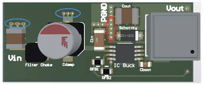
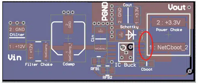
To further reduce the potential noise from a high ΔI/Δt, it is essential to place the input capacitor very close to the Vin pin (drain connection of the internal or external high-side MOSFET) of the buck regulator.
In combination with the “Single Point PGND” ground reference, a very small current loop is obtained and therefore also a small parasitic H-field loop (loop antenna). A very high ΔI/Δt also occurs in the bootstrap circuit. Therefore, it is important to place the bootstrap capacitor directly at the associated buck regulator pin.
To keep undesirable output voltage fluctuations low, the feedback resistor network should also be placed close to the regulator. The possibly very long feedback trace therefore has a low impedance and is less sensitive to interference. The output voltage for regulation should be tapped at a point as close to the output capacitor as possible.
To transfer theory into practice, here is a sample calculation:
Example Buck Converter Design and Calculation
storage inductor of an asynchronous buck converter
Input voltage: Vin = 12 V nominal
Output voltage: Vout = 3.3 V
Output current: Iout = 1 A max.
Switching frequency: fsw = 500 kHz
Max. bandwidth control loop/crossover frequency: fc = 10 kHz
Forward voltage rectifier diode: VD = 0.4 V
Ripple current factor: r = ΔI/Iout ≈ 0.35
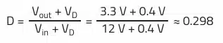
Duty cycle D:
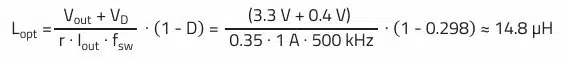
Minimum inductance necessary to maintain ripple current factor:
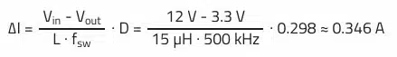
Considering a standard inductance value of 15 µH, this results in a ripple current of:
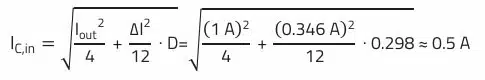
Rated Current Ir:
Often it is sufficient to select the rated current based on the average inductor current (output current at the buck converter) with some margin. In fact, the RMS value of the inductor current (average inductor current + AC ripple current) is responsible for the heat generated at the DC resistor (see RMS chapter in Selection of Storage Inductors for DC/DC Converters).
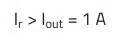
A choke with more than 1 A rated current (according to datasheet) should be selected.
Saturation Current Isat:
Half the AC ripple current must be added to the average inductor current to determine the maximum peak current. The average inductor current of the buck converter corresponds to the output current.
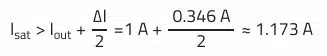
Now a suitable storage choke based on these results can be selected. Some safety margin should also be included, as component tolerance and ambient temperature have been neglected here. For this example, an experienced designer selects an inductor with at least 15 µH according to the datasheet, as well as 1.1 A rated current and 1.5 A saturation current.
Practical Inductor Selection for Buck Converters
Once the required inductance, rated current and saturation current have been calculated as shown above, those values must be translated into a real inductor that will operate safely over the full input-voltage and load range. The following selection procedure — illustrated with a second, higher-current example — shows how to do this systematically.
Step 1 — Define the operating window
Before searching a datasheet, fix the six key parameters:
- Maximum input voltage V_in,max
- Minimum input voltage V_in,min
- Maximum output current I_out,max
- Minimum output current I_out,min
- Output voltage V_out
- Switching frequency f_sw
For a typical automotive buck stage: f_sw = 500 kHz, V_out = 5 V, I_out,max = 4 A, I_out,min = 0.5 A, V_in,max = 13.5 V, V_in,min = 8.5 V.
Step 2 — Determine minimum duty cycle and inductance
The minimum duty cycle occurs at maximum input voltage:
D_min = V_out / V_in,max
The minimum inductance required to keep the inductor current continuous down to the minimum load (so that the current ripple just touches zero at I_out,min) is found from the standard buck inductance formula applied at the worst-case condition. For the automotive example this yields a required inductance of approximately 8.2 µH.
Step 3 — Calculate ripple current, peak current and RMS current
With the inductance fixed, the key current parameters are:
- Ripple current ΔI — sets the peak-to-peak swing; also drives output voltage ripple via the ESR of the output capacitor. High ripple increases core losses; low ripple requires a larger inductor.
- Peak current I_pk = I_out,avg + ΔI/2 — the inductor must not saturate at this value.
- RMS current I_rms ≈ √(I_out,avg² + ΔI²/12) — drives ohmic (I²R) heating in the winding.
For the automotive example: I_pk ≈ 4.42 A, I_rms ≈ 4.0 A.
Step 4 — Match a real part to the calculated requirements
The chosen inductor must satisfy three conditions simultaneously:
| Parameter | Requirement | Typical margin |
|---|---|---|
| Nominal inductance L | ≥ calculated minimum | Use nearest standard value |
| Saturation current I_sat (30% roll-off) | > I_pk | +20…30% recommended |
| Rated current I_r (thermal limit) | > I_rms | Verify temperature rise curve |
Step 5 — Verify with DC-bias and temperature-rise curves
Datasheet graphs for inductance vs. DC bias and temperature rise vs. DC current are the key verification tools. Note that the temperature-rise curve is specified for pure DC current. In a buck converter the inductor also carries AC ripple current, so actual losses and temperature rise will be somewhat higher. A precise thermal estimate must account for:
- Skin depth at the switching frequency and effective conductor cross-section
- Surface area and thermal environment of the inductor package
- DC winding resistance at the expected operating temperature
- AC flux density B_AC, derived from peak current, inductance, core cross-sectional area and number of turns
These parameters are best handled with manufacturer loss models or simulation tools; see the REDEXPERT workflow described in the next section.
Scaling Buck Inductor Selection to AI Server VRMs
The same five-step procedure scales directly to the multiphase buck stages used in AI server voltage regulator modules (VRMs) — just at far higher current and phase counts. Modern GPU power delivery still selects inductors on inductance, saturation current and RMS current, but now at 45–160 A per phase across 48–56 phases per GPU, versus 8–12 phases in the H100 generation. Trans-inductor voltage regulator (TLVR) architectures add magnetic coupling between phases, which extends control bandwidth enough to use a smaller inductance value while still meeting transient targets:
A closer look at these multiphase and TLVR buck architectures — including voltage-layer mapping and 2026 supply trends for AI hardware — is covered in our AI Hardware Passive Components Dossier.
| Parameter | Standard Multiphase Buck | TLVR Architecture |
|---|---|---|
| Transient response bandwidth | Limited by L_out | Extended by phase coupling (3–5× faster) |
| Output capacitance required | 100% baseline | ~50% reduction possible |
| Current ramp speed | 1× baseline | 3–5× faster |
| Phase count (GPU VRM) | 8–12 phases (H100 era) | 48–56 phases (Rubin era) |
| Inductance range | 100–560 nH | 70–200 nH (±10–15% tolerance) |
| Saturation current | 20–60 A per phase | 45–160 A per phase (Bourns TLVR1005T) |
| DCR (typical) | 0.5–2 mΩ | 0.125–0.450 mΩ (Bourns TLVR series) |
Sources: APEC 2026 Infineon TDM24745T, Bourns TLVR1005T/TLVR1105T datasheet, NIC Components NLVR series.
Input Capacitor for a Buck Converter
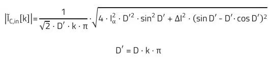
RMS current (ripple current) through the input capacitor:
With the help of the REDEXPERT tool, a capacitor can now be selected with the lowest possible impedance at the switching frequency of 500 kHz, which at the same time meets the requirements in terms of ripple current as well as voltage.
Output Capacitor for a Buck Converter
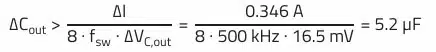
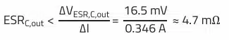
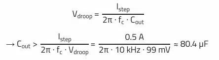
The output capacitor is defined based on the maximum permissible voltage ripple and based on the maximum permissible voltage change (Vdroop) resulting from a load step. In our example, we want to allow a maximum of 1% residual voltage ripple, i.e., 33 mV at an output voltage of 3.3 V and only 3% voltage dip, corresponding to 99 mV, at a load step (Istep = 0.5 A) from 0.5 to 1 A.
From these assumptions, the minimum necessary capacitance can be calculated, which fulfills both requirements. For the output voltage residual ripple, in addition to the capacitance-dependent part, the influence of the ESR is considered (the ESL is neglected). For simplicity, an even split is assumed for the two components, resulting in 16.5 mV each for the capacitance and the ESR calculations.
In addition, it must be checked mathematically whether the AC current through the output capacitor stays below the maximum ripple current according to the data sheet.
The following equation describes the relationship between the output capacitance and the ripple voltage for a buck converter topology (assumption: ideal capacitor):
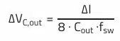
The next equation is used to calculate the minimum capacitance required for the given capacitance dependent ripple:
The next equation describes the relationship between the ESR of the output capacitor and the ripple voltage for a buck converter topology (assumption: ESL is neglected):
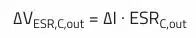
This equation is used to calculate the maximum allowable ESR of the output capacitor based on the given ESR-dependent ripple voltage:
This equation is used to calculate the minimum output capacitance to maintain a given voltage droop during a load step:
The next equation is used to determine the RMS current that flows through the output capacitor of the buck converter:
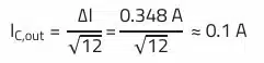
The capacitance of 5.2 µF for the maximum defined voltage ripple is not relevant in this case, as the minimum necessary capacitance of 80.4 µF results from the maximum allowed voltage change during load transients. Based on the calculated results, we therefore need a capacitor with at least 82…100 µF (standard values).
The ESR could be higher than 4.7 mΩ since the capacitance-dependent part of the ripple is lower due to the higher capacitance value. An H-chip polymer SMT capacitor, such as the WCAP-PHLE (875035019001), would be a suitable choice for this purpose. This offers a stable capacitance of 100 µF in a very small package (7.3 · 4.3 · 1.9 mm³), a 3.5 mΩ low ESR at 500 kHz and it is specified for a ripple current of up to 6.3 A.
Design of the Input Filters for a Buck Converter
The switching regulator operates at 12 V and 500 kHz. In chapter 1.4.2 it was mentioned that it makes sense to design the cut-off frequency of the LC input filter to 1/10 of the switching frequency. This provides about 40 dB attenuation for the fundamental wave (switching frequency).
A 22 µF/25 V/MLCC or polymer (advantage of polymer = stable capacitance, no DC bias effect as with class 2 MLCCs) type is specified as filter capacitor. The following formula can now be used to calculate the necessary filter inductance.
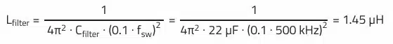
The next possible default value, 1.5 µH nominal, is selected. The rated and saturation current of the filter inductor should be approx. 20…40% above the maximum DC input current of the converter.
Design of the Output Filters for a Buck Converter
In some applications, there is the necessity to filter the output again. Like at the input of the converter, an LC filter with a small inductance is suitable for this purpose. Alternatively, or additionally, a pulse current-resistant multilayer power suppression ferrite WE-MPSB can be used.
The calculation is carried out in the same way as for the input filter. Due to the higher current at the output of a buck converter, the filter inductance should remain as small as possible in relation to the filter capacitor (e.g., 1:10 ➔ 1 µH : 10 µF) to keep the efficiency as high as possible.
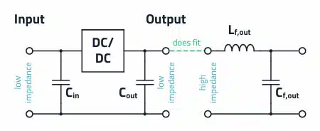
Important: The feedback tap of the output voltage for the control loop must still take place at the actual output capacitor, and not at the filter capacitor! But there are applications, especially for high current PoL buck converters, where the voltage drop across the filter inductance cannot be ignored. In this case, the feedback tap must be after the filter inductance, so the voltage drop, due to the RDC, can be readjusted. Special restrictions apply to this circuit version, which are described in more detail in Application Note ANP044 “Impact of the layout, components, and filters on the EMC of modern DC/DC switching controllers“ (www.we-online.com/ANP044).
Read also the related articles in this series:
For a broader, application-driven view of how capacitor, inductor, resistor, EMI and protection choices differ across buck, boost, flyback, LLC and other topologies in automotive, AI data-center, industrial and renewable systems, see our Passive Components for Power Converters Dossier.
- Selection of Capacitors for DC/DC Converters
- Selection of Storage Inductors for DC/DC Converters
- Input filters for DC/DC converters
- Switching vs Linear Power Converters Compared
- SEPIC Converter Design and Calculation
- Boost Converter Design and Calculation
- Flyback Converter Design and Calculation
- Fly-Buck Converter Explained and Comparison to Flyback
- LLC Resonant Converter Design and Calculation
Buck and Boost Converter Basic Formulas
The following table 1. provides basic formulas of the buck and boost converter topologies.
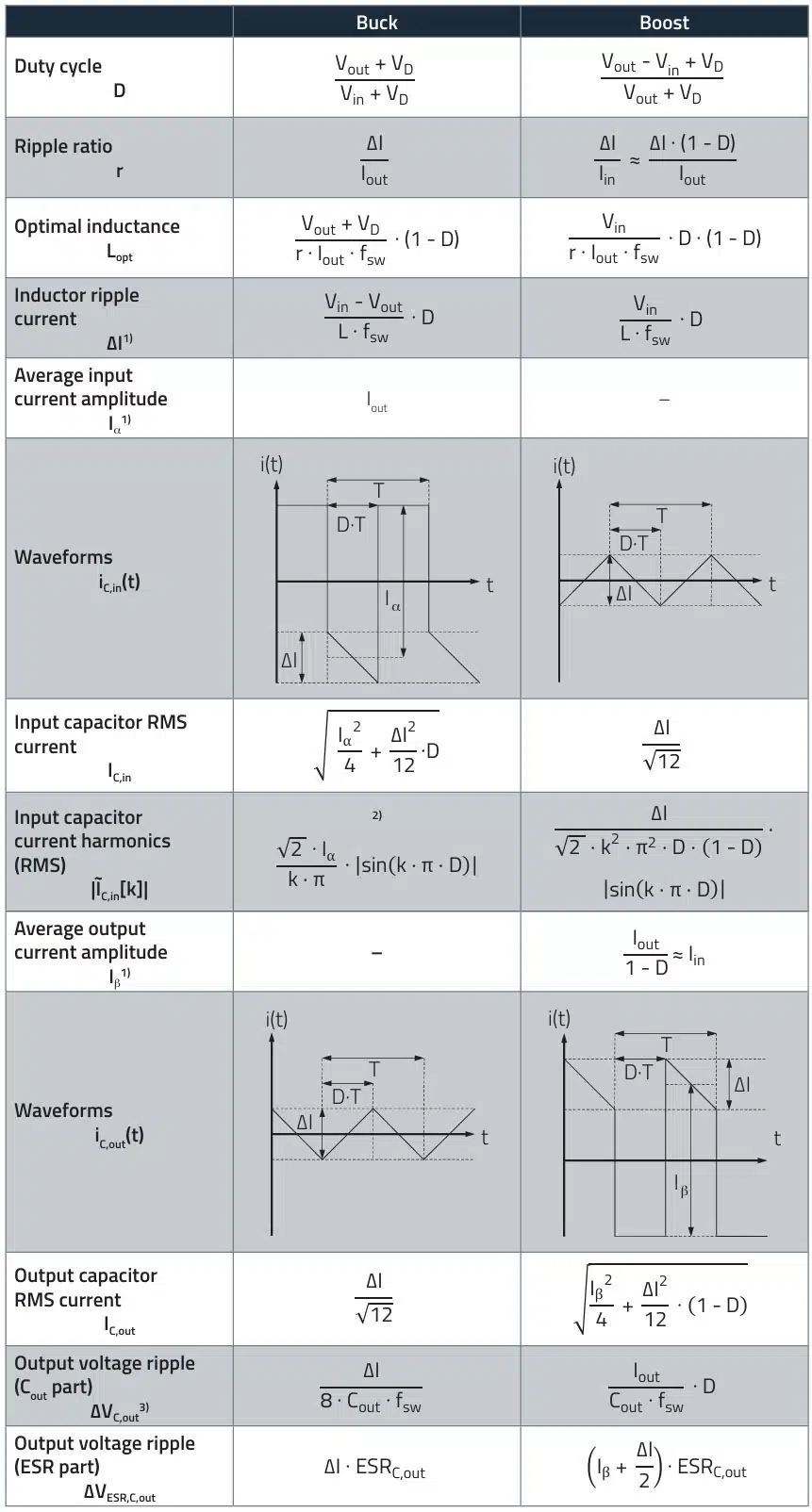
1) These assumptions apply to the ideal switching regulator in continuous conduction mode
(CCM), i.e., the efficiency of the converter is assumed to be 100% (η = 1).
2) The current curve from this equation is approximately rectangular (ΔI neglected). Exactly:
3) The equations defined for ΔVC,out apply to the ideal capacitor. Cout therefore defines the minimum capacitance to meet the ripple voltage requirement. The actual voltage ripple will be higher due to the parasitic inductance ESL (equivalent series inductance) and ESR (equivalent series resistance) of the capacitor.
FAQ: Buck Converter
A buck converter steps down a higher DC input voltage to a lower DC output voltage with high efficiency, making it ideal for regulated power supplies in telecommunications, automotive, medical and industrial applications.
Improper layout increases parasitic inductance and capacitance, leading to EMI issues, voltage ripple and reduced efficiency. Keeping the high ΔI/Δt loops compact and minimizing the hot node area are the two most impactful layout rules.
Start by calculating the minimum inductance, peak current and RMS current from the operating parameters. Then choose a real part whose nominal inductance meets the minimum value, whose saturation current (at 30% roll-off) exceeds the peak current with a 20–30% margin, and whose rated current exceeds the RMS current. Always verify both the DC-bias inductance curve and the temperature-rise curve from the datasheet. For automotive-grade designs, use AEC-Q200 qualified parts.
The output capacitor must balance capacitance and ESR to satisfy both the steady-state ripple voltage requirement and the transient voltage droop during load steps. In the 12 V→3.3 V / 1 A example, at least 82–100 µF with ESR below 4.7 mΩ at 500 kHz was required for stable operation.
Rated current (I_r) is the thermal limit — the DC current at which the inductor reaches a specified temperature rise (typically 40 °C). Saturation current (I_sat) is the magnetic limit — the DC current at which inductance drops by a defined percentage (typically 20–30%). In a buck converter, I_r must exceed the RMS inductor current and I_sat must exceed the peak inductor current.
How to Design a Buck Converter
- Define Requirements
Set input voltage range (min and max), output voltage, maximum and minimum output current, and switching frequency.
- Calculate Duty Cycle
Use D = V_out / V_in (corrected for diode drop in asynchronous designs) to determine the operating duty cycle range.
- Calculate Minimum Inductance
Apply the buck inductance formula at the worst-case condition (maximum input voltage, minimum load) using the chosen ripple current factor (typically r = ΔI/I_out ≈ 0.3–0.4). Select the nearest standard inductance value above the calculated minimum.
- Select the Inductor
Fix the six operating-window parameters (V_in,max, V_in,min, I_out,max, I_out,min, V_out, f_sw).
Calculate ripple current ΔI, peak current I_pk and RMS current I_rms.
Choose a part with nominal L ≥ calculated minimum, I_sat > I_pk (+20–30% margin) and I_r > I_rms.
Verify with the datasheet DC-bias inductance curve and temperature-rise curve.
For safety-critical or automotive designs, select AEC-Q200 qualified inductors. - Choose Input and Output Capacitors
The input capacitor must handle the discontinuous RMS ripple current. The output capacitor must satisfy both the steady-state ripple voltage (capacitance and ESR limits) and the transient voltage droop specification during load steps.
- Optimize PCB Layout
Minimize the hot node area to reduce E-field radiation. Place the input capacitor as close as possible to the MOSFET drain pin. Use a single-point power ground (PGND) to minimize H-field loops. Orient filter inductors and capacitors at 90° to each other to avoid magnetic coupling.
- Design Input Filter
Size the LC input filter cut-off frequency to 1/10 of the switching frequency for approximately 40 dB attenuation at the fundamental. Rate the filter inductor 20–40% above the maximum DC input current.
- Design Output Filter (if required)
Use a small LC filter (e.g., 1 µH : 10 µF ratio) if low residual ripple is needed. Keep the feedback voltage tap at the main output capacitor, not at the filter capacitor, unless PoL voltage-drop compensation is applied.
- Validate with Simulation
Use tools like REDEXPERT to confirm inductor and capacitor ratings under the actual AC + DC operating conditions, and to account for losses beyond the DC-only datasheet curves.